SFFS183A March 2022 – August 2025 LMR43610 , LMR43610-Q1 , LMR43620 , LMR43620-Q1
4 Pin Failure Mode Analysis (Pin FMA)
This section provides a failure mode analysis (FMA) for the pins of the LMR436x0 and LMR436x0-Q1. The failure modes covered in this document include the typical pin-by-pin failure scenarios:
- Pin short-circuited to ground (see Table 4-2)
- Pin open-circuited (see Table 4-3)
- Pin short-circuited to an adjacent pin (see Table 4-4)
- Pin short-circuited to supply (see Table 4-5)
Table 4-2 through Table 4-5 also indicate how these pin conditions can affect the device as per the failure effects classification in Table 4-1.
| Class | Failure Effects |
|---|---|
| A | Potential device damage that affects functionality. |
| B | No device damage, but loss of functionality. |
| C | No device damage, but performance degradation. |
| D | No device damage, no impact to functionality or performance. |
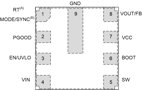
Figure 4-1 shows the LMR436x0 and LMR436x0-Q1 pin diagram. For a detailed description of the device pins please refer to the Pin Configuration and Functions section in the LMR436x0 and LMR436x0-Q1 data sheet.
 Figure 4-1 Pin Diagram
Following are the assumptions of use and the device configuration assumed for the pin FMA in this section:
- Application circuit, as per the LMR436x0 and LMR436x0-Q1 data sheets is used.
| Pin Name | Pin No. | Description of Potential Failure Effects | Failure Effect Class |
|---|---|---|---|
| RT or MODE/SYNC | 1 | The switching frequency is 2.2MHz. | D |
| PGOOD | 2 | When not in use, this pin can be left grounded (PGOOD is not a valid signal and VOUT is normal). | D |
| EN/UVLO | 3 | VOUT = 0V. (Enable is off and functionality is halted.) | D |
| VIN | 4 | VOUT = 0V. | B |
| SW | 5 | Damage to the HS FET. | A |
| BOOT | 6 | VOUT = 0V. HS does not turn on. | B |
| VCC | 7 | VOUT = 0V. | B |
| VOUT/BIAS or FB | 8 | When in adjustable output mode, VOUT approaches VIN. When in fixed output mode, VOUT = 0V. | B |
| GND | 9 | VOUT is normal. | D |
| Pin Name | Pin No. | Description of Potential Failure Effects | Failure Effect Class |
|---|---|---|---|
| RT or MODE/SYNC | 1 | If an RT part, frequency is not defined. If a MODE/SYNC part, then the part can go back and forth between FPWM/PFM. The part is up and functional. | C |
| PGOOD | 2 | When not in use, this pin can be left open (PGOOD is not a valid signal and VOUT is normal). | D |
| EN/UVLO | 3 | Pin cannot be left floating. | B |
| VIN | 4 | VOUT = 0V. | B |
| SW | 5 | VOUT = 0V. | B |
| BOOT | 6 | VOUT = 0V. HS does not turn on. | B |
| VCC | 7 | VCC output is unstable and can increase above 5.5V. | A |
| VOUT/BIAS or FB | 8 | VOUT approaches VIN. | C |
| GND | 9 | VOUT can be abnormal, as reference voltage is not fixed. | C |
| Pin Name | Pin No. | Shorted to | Description of Potential Failure Effects | Failure Effect Class |
|---|---|---|---|---|
| RT or MODE/SYNC | 1 | PGOOD | If PGOOD is high, and < 5.5V, FSW = 1MHz. If PGOOD is low, FSW = 2.2MHz. With PGOOD absolute maximum rating being 20V, RT ESD damages if PG goes to 20V. | A |
| PGOOD | 2 | EN/UVLO | If EN/UVLO > 20V, damages devices connected to the PGOOD pin. | A |
| EN/UVLO | 3 | VIN | VOUT is normal (Enable is on and all other blocks work). | D |
| VIN | 4 | SW | Damage to LS FET. | A |
| SW | 5 | BOOT | VOUT = 0V. HS does not turn on and there is no CBOOT. | B |
| BOOT | 6 | VCC | Damage occurs and there is a break to the VCC pin. | A |
| VCC | 7 | VOUT/BIAS or FB | Does not work, but no damage occurs. | B |
| VOUT/BIAS or FB | 8 | GND | When in adjustable output mode, VOUT approaches VIN. When in fixed output mode, VOUT = 0V. | B |
| GND | 9 | RT or MODE/SYNC | VOUT is normal if the RT/MODE/SYNC pin is low, otherwise not functional. | B |
| Pin Name | Pin No. | Description of Potential Failure Effects | Failure Effect Class |
|---|---|---|---|
| RT or MODE/SYNC | 1 | If VIN > 5.5V, damage occurs. If VIN < 5.5V, switching frequency is 1MHz. | A |
| PGOOD | 2 | If VIN > 20V, damages PGOOD. | A |
| EN/UVLO | 3 | VOUT is normal (Enable is on and all other blocks work). | D |
| VIN | 4 | VOUT is normal. | D |
| SW | 5 | Damage to LS FET. | A |
| BOOT | 6 | Damage occurs and BOOT ESD clamp is damaged. | A |
| VCC | 7 | If VIN > 5.5V, damage occurs. | A |
| VOUT/BIAS or FB | 8 | If VIN > 16V, damage occurs. | A |
| GND | 9 | VOUT = 0V. | B |