SFFS025 March 2021 TLIN1029A-Q1
4 Pin Failure Mode Analysis (Pin FMA)
This section provides a Failure Mode Analysis (FMA) for the pins of the TLIN1029A-Q1. The failure modes covered in this document include the typical pin-by-pin failure scenarios:
- Pin short-circuited to Ground (see Table 4-2)
- Pin open-circuited (see Table 4-3)
- Pin short-circuited to an adjacent pin (see Table 4-4)
- Pin short-circuited to supply (see Table 4-5)
Table 4-2 through Table 4-5 also indicate how these pin conditions can affect the device as per the failure effects classification in Table 4-1.
| Class | Failure Effects |
|---|---|
| A | Potential device damage that affects functionality |
| B | No device damage, but loss of functionality |
| C | No device damage, but performance degradation |
| D | No device damage, no impact to functionality or performance |
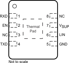
Figure 4-1 shows the device pin diagram. For a detailed description of the device pins, please refer to the Pin Configuration and Functions section in the TLIN1029A-Q1 data sheet.
 Figure 4-1 DRB Pin Diagram
 Figure 4-2 D Pin Diagram
Following are the assumptions of use and the device configuration assumed for the pin FMA in this section:
- All conditions within the recommended operating conditions
| Pin Name | Pin No. | Description of Potential Failure Effect(s) | Failure Effect Class |
|---|---|---|---|
| RXD | 1 | RXD biased dominant, no communication from LIN bus to MCU possible | B |
| EN | 2 | Device may only operate in Standby Mode after power-on. If short occures in Normal mode, the part would be forced to enter sleep mode and could disable LIN communication | B |
| NC | 3 | No impact to performance | D |
| TXD | 4 | TXD biased dominant, no communication from MCU to LIN bus possible | B |
| GND | 5 | None | D |
| LIN | 6 | LIN biased dominant, no LIN communication possible | B |
| VSUP | 7 | Device is unpowered and will not function | B |
| NC | 8 | No impact to performance | D |
| Pin Name | Pin No. | Description of Potential Failure Effect(s) | Failure Effect Class |
|---|---|---|---|
| RXD | 1 | No communication from LIN bus to MCU possible | B |
| EN | 2 | Biased low due to internal pull-down so device in standby mode | B |
| NC | 3 | No impact to performance | D |
| TXD | 4 | No communication from MCU to LIN bus possible | B |
| GND | 5 | Device is unpowered and will not function | B |
| LIN | 6 | No LIN communication possible | B |
| VSUP | 7 | Device is unpowered and will not function | B |
| NC | 8 | No impact to performance | D |
| Pin Name | Pin No. | Shorted to | Description of Potential Failure Effect(s) | Failure Effect Class |
|---|---|---|---|---|
| RXD | 1 | EN | Device will go into sleep mode when a dominant bit is received on the LIN bus, disabling communication | B |
| EN | 2 | NC | No impact to performance | D |
| NC | 3 | TXD | No impact to performance | D |
| GND | 5 | LIN | LIN biased dominant, no LIN communication possible | B |
| LIN | 6 | VSUP | LIN biased recessive, no LIN communication possible | B |
| VSUP | 7 | NC | No impact to performance | D |
| Pin Name | Pin No. | Description of Potential Failure Effect(s) | Failure Effect Class |
|---|---|---|---|
| RXD | 1 | Absolute maximum voltage violation, transceiver may be damaged | A |
| EN | 2 | Absolute maximum voltage violation, transceiver may be damaged | A |
| NC | 3 | No impact to performance | D |
| TXD | 4 | Absolute maximum voltage violation, transceiver may be damaged | A |
| GND | 5 | Device is unpowered and will not function | B |
| LIN | 6 | LIN biased recessive, no LIN communication possible | B |
| VSUP | 7 | None | D |
| NC | 8 | No impact to performance | D |