SDAA192 November 2025 UCC33020 , UCC33020-Q1 , UCC33410 , UCC33410-Q1 , UCC33420 , UCC33420-Q1
2.4 Faraday Shield
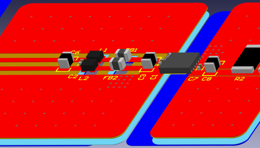
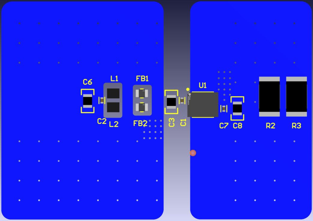
PCB Faraday shield is a technique used to mitigate the H filed coming from the integrated transformer. It consists on placing conductive copper from an inner or bottom layer underneath the device. This Faraday shield induces currents that generate a H field of the opposite direction than the original one. To prevent any bypass of these induced currents, we also recommend having an approximate 4mm clearance between the primary and secondary ground planes. This is achieved by pulling back the primary ground plane 4mm from the extended secondary ground plane. In a 2-layer PCB, this clearance is needed to keep isolation requirements. In a 4-layer PCB, the Faraday shield can be placed in an inner layer but the 4mm clearance is still required. The frequency target of this shield is between 500MHz-1GHz.
 Figure 2-18 3D View of the Faraday
Shield
 Figure 2-19 2D View of the Faraday
Shield