ZHCSID4B June 2018 – January 2021 TPS61372
PRODUCTION DATA
- 1 特性
- 2 應用
- 3 說明
- 4 Revision History
- 5 Pin Configuration and Functions
- 6 Specifications
- 7 Detailed Description
-
8 Application and Implementation
- 8.1 Application Information
- 8.2
Typical Application
- 8.2.1 Design Requirements
- 8.2.2
Detailed Design Procedure
- 8.2.2.1 Custom Design With WEBENCH? Tools
- 8.2.2.2 Setting the Output Voltage
- 8.2.2.3 Selecting the Inductor
- 8.2.2.4 Selecting the Output Capacitors
- 8.2.2.5 Selecting the Input Capacitors
- 8.2.2.6 Loop Stability and Compensation
- 8.2.2.7 Loop Compensation Design Steps
- 8.2.2.8 Selecting the Bootstrap Capacitor
- 8.2.3 Application Curves
- 9 Power Supply Recommendations
- 10Layout
- 11Device and Documentation Support
- 12Mechanical, Packaging, and Orderable Information
封裝選項
請參考 PDF 數(shù)據(jù)表獲取器件具體的封裝圖。
機械數(shù)據(jù) (封裝 | 引腳)
- YKB|16
散熱焊盤機械數(shù)據(jù) (封裝 | 引腳)
訂購信息
5 Pin Configuration and Functions
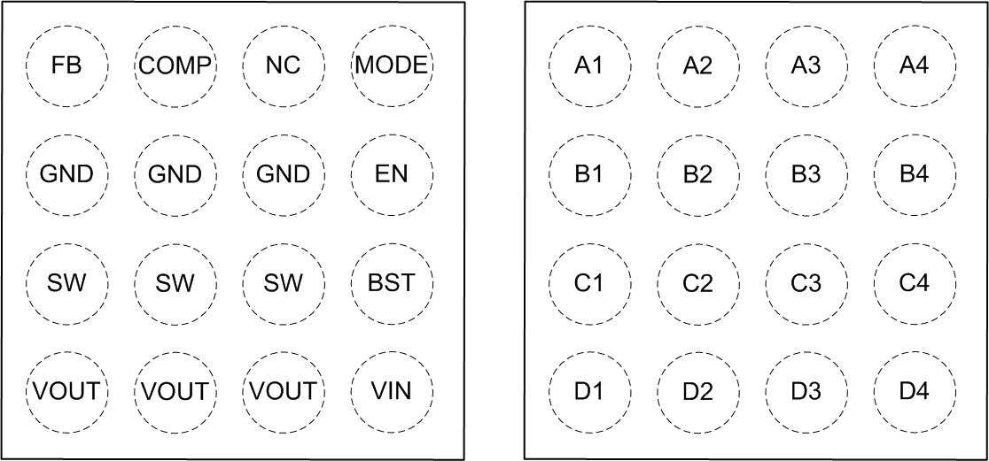
 Figure 5-1 YKB
Package16-Pin DSBGA
(Top View)
Figure 5-1 YKB
Package16-Pin DSBGA
(Top View)Table 5-1 Pin Functions
| PIN | I/O | DESCRIPTION | |
|---|---|---|---|
| NUMBER | NAME | ||
| A1 | FB | I | Output voltage feedback. A resistor divider connecting to this pin sets the output voltage. |
| A2 | COMP | O | Output of the internal error amplifier. The loop compensation network must be connected between this pin and GND. |
| A3 | NC | I | No connection. Tie directly to VIN pin. Do not connect with GND or leave it floating. |
| A4 | MODE | I | Operation mode selection pin. MODE = low, the device works in auto PFM mode with good light load efficiency. MODE = high, the device is in forced PWM mode and keeps the switching frequency constant across the whole load range. |
| B1, B2, B3 | GND | - | Ground |
| B4 | EN | I | Enable logic input. Logic high level enables the device. Logic low level disables the device and turns it into shutdown mode. |
| C1, C2, C3 | SW | PWR | The switching node pin of the converter. It is connected to the drain of the internal low-side FET and the source of the internal high-side FET. |
| C4 | BST | O | Power supply for the high-side FET gate driver. A capacitor must be connected between this pin and the SW pin. |
| D1, D2, D3 | VOUT | PWR | Boost converter output |
| D4 | VIN | I | IC power supply input |