ZHCSD74A January 2014 – December 2014 TPS61097A-33
PRODUCTION DATA.
- 1 特性
- 2 應(yīng)用
- 3 說明
- 4 修訂歷史記錄
- 5 Pin Configuration and Functions
- 6 Specifications
- 7 Parameter Measurement Information
- 8 Detailed Description
- 9 Application and Implementation
- 10Power Supply Recommendations
- 11Layout
- 12器件和文檔支持
- 13機(jī)械封裝和可訂購信息
封裝選項
機(jī)械數(shù)據(jù) (封裝 | 引腳)
- DBV|5
散熱焊盤機(jī)械數(shù)據(jù) (封裝 | 引腳)
訂購信息
6 Specifications
6.1 Absolute Maximum Ratings
Over operating free-air temperature range (unless otherwise noted)(1)| MIN | MAX | UNIT | |||
|---|---|---|---|---|---|
| VI | Input voltage range | VIN | –0.3 | 7 | V |
| L | –0.3 | 7 | |||
| VOUT | –0.3 | 7 | |||
| EN | –0.3 | 7 | |||
| IMAX | Maximum continuous output current | 400 | mA | ||
| TJ | Junction temperature range | –40 | 150 | °C | |
| Tstg | Storage temperature range | –65 | 150 | °C | |
(1) Stresses beyond those listed under Absolute Maximum Ratings may cause permanent damage to the device. These are stress ratings only, and functional operation of the device at these or any other conditions beyond those indicated under Recommended Operating Conditions is not implied. Exposure to absolute-maximum-rated conditions for extended periods may affect device reliability.
6.2 ESD Ratings
| VALUE | UNIT | |||
|---|---|---|---|---|
| V(ESD) | Electrostatic discharge | Human-body model (HBM), per ANSI/ESDA/JEDEC JS-001(1) | ±2000 | V |
| Charged-device model (CDM), per JEDEC specification JESD22-C101(2) | ±1000 | |||
(1) JEDEC document JEP155 states that 500-V HBM allows safe manufacturing with a standard ESD control process.
(2) JEDEC document JEP157 states that 250-V CDM allows safe manufacturing with a standard ESD control process.
6.3 Recommended Operating Conditions
| MIN | MAX | UNIT | ||
|---|---|---|---|---|
| VIN | Input voltage range | 0.9 | 5.5 | V |
| VEN | Enable voltage range | 0 | 5.5 | V |
| TA | Operating free air temperature range | –40 | 85 | °C |
| TJ | Operating junction temperature range | –40 | 125 | °C |
6.4 Thermal Information
| THERMAL METRIC(1) | TPS61097A-33 | UNIT | |
|---|---|---|---|
| DBV | |||
| 5 PINS | |||
| θJA | Junction-to-ambient thermal resistance | 208.7 | °C/W |
| θJCtop | Junction-to-case (top) thermal resistance | 124.5 | |
| θJB | Junction-to-board thermal resistance | 36.9 | |
| ψJT | Junction-to-top characterization parameter | 14.7 | |
| ψJB | Junction-to-board characterization parameter | 36 | |
(1) For more information about traditional and new thermal metrics, see the IC Package Thermal Metrics application report, SPRA953.
6.5 Electrical Characteristics
Over recommended free-air temperature range and over recommended input voltage range (typical at an ambient temperature range of 25°C) (unless otherwise noted)| PARAMETER | TEST CONDITIONS | MIN | TYP | MAX | UNIT | ||||
|---|---|---|---|---|---|---|---|---|---|
| DC/DC STAGE | |||||||||
| VIN | Input voltage | 0.9 | 5.5 | V | |||||
| VOUT | Output voltage | VIN = 1.2 V , IOUT = 10 mA | 3.20 | 3.30 | 3.40 | ||||
| ISW | Switch current limit | VOUT = 3.3 V | 200 | 400 | 475 | mA | |||
| Rectifying switch on resistance | VOUT = 3.3 V | 1.0 | Ω | ||||||
| Main switch on resistance | VOUT = 3.3 V | 1.0 | |||||||
| Bypass switch on resistance | VIN = 1.2 IOUT = 100 mA | 3.4 | |||||||
| Line regulation | VIN < VOUT, VIN = 1.2 V to 1.8 V, IOUT = 10 mA | 0.5% | |||||||
| Load regulation | VIN < VOUT, IOUT = 10 mA to 50 mA, VIN = 1.8 V | 0.5% | |||||||
| IQ | Quiescent current | VIN | IOUT = 0 mA, VEN = VIN = 1.2 V, VOUT = 3.5 V | 2 | 4 | μA | |||
| VOUT | 5 | 8 | |||||||
| ISD | Shutdown current | VIN | VEN = 0 V, VIN = 1.2 V, IOUT = 0 mA | 0.005 | 0.15 | μA | |||
| VEN = 0 V, VIN = 3 V, IOUT = 0 mA | 0.005 | 0.15 | |||||||
| Leakage current into L | VEN = 0 V, VIN = 1.2 V, VL = 1.2 V | 0.01 | 1 | ||||||
| CONTROL STAGE | |||||||||
| EN input current | EN = 0 V or EN = VIN | 0.01 | 0.1 | μA | |||||
| VIL | Logic low level, EN falling edge | 0.58 | V | ||||||
| VIH | Logic high level, EN rising edge | 0.78 | VIN + 1.0 V | ||||||
| OTP | Overtemperature protection | 150 | °C | ||||||
| OTPHYST | Overtemperature hysteresis | 20 | |||||||
| VUVLO | Undervoltage lock-out threshold for turn off | VIN decreasing | 0.6 | 0.8 | V | ||||
6.6 Typical Characteristics
Refer to Figure 19 for reference designators.
 Figure 1. Maximum Output Current vs Input Voltage
 Figure 3. Efficiency vs Input Voltage
 Figure 5. Input Current vs Input Voltage
 Figure 7. VIH vs Output Current
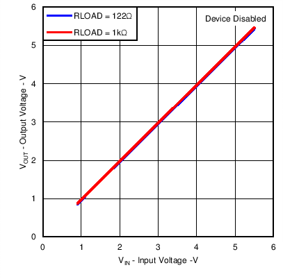 Figure 9. Output Voltage vs Input Voltage
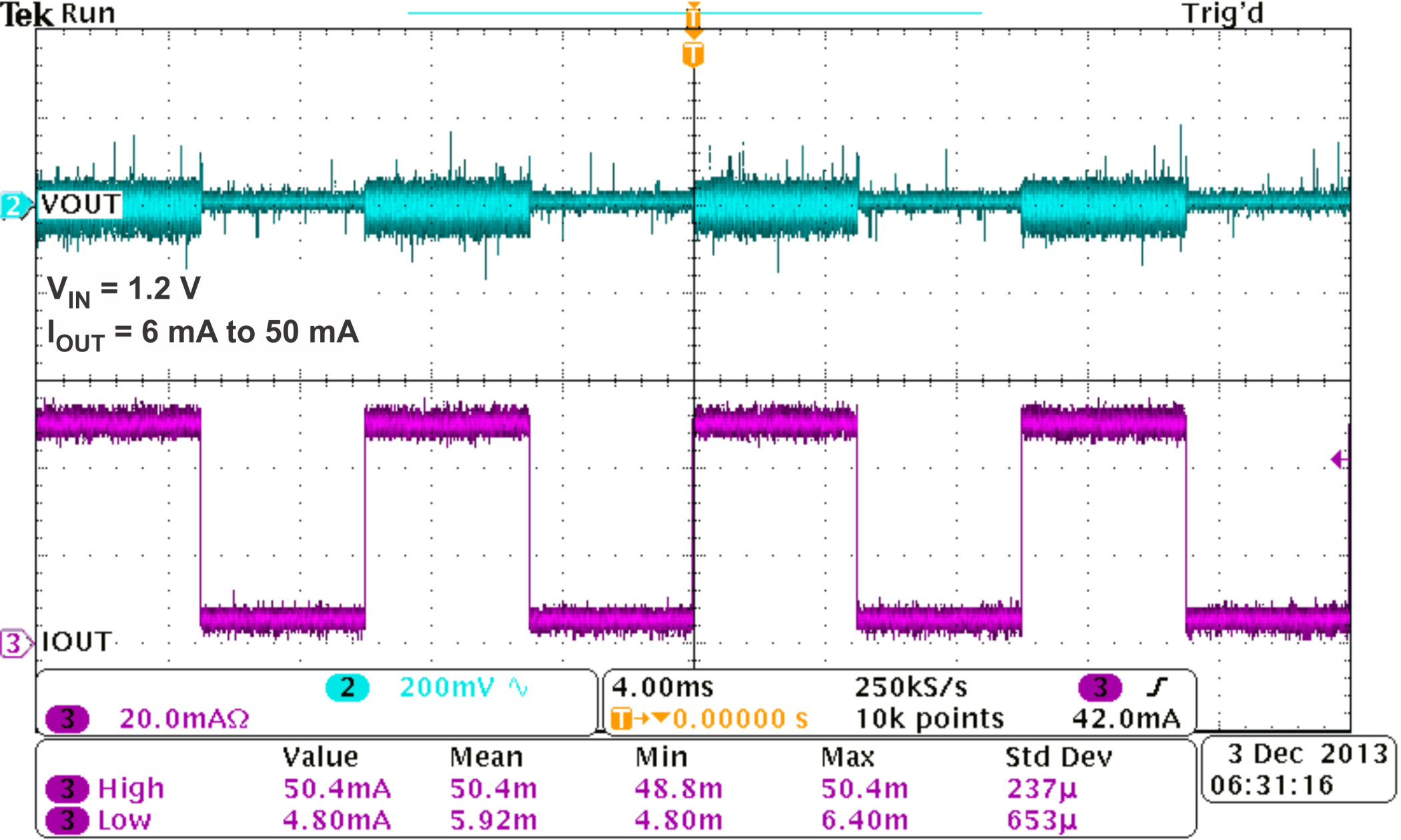 Figure 11. Load Transient Response
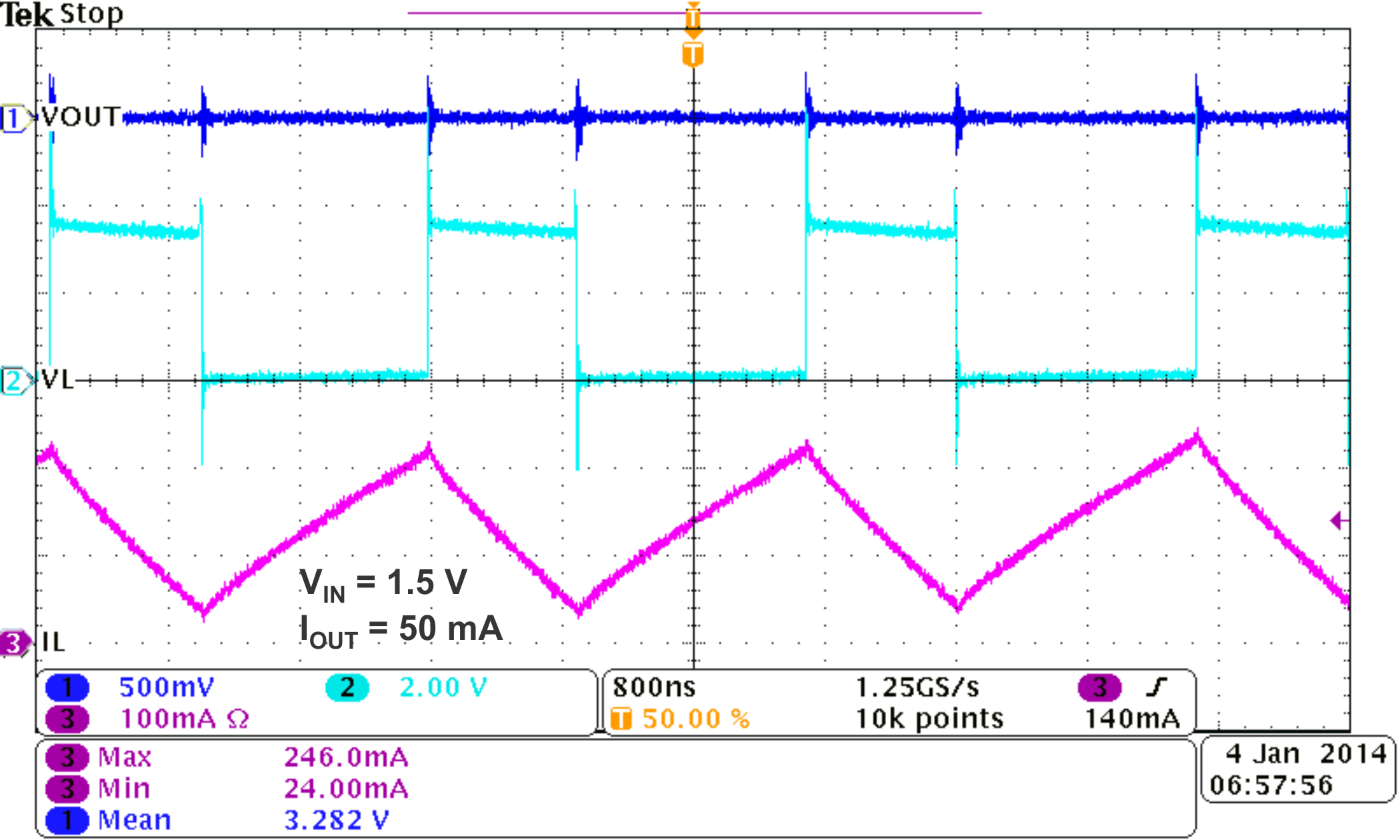 Figure 13. Switching Waveform, Continuous Mode
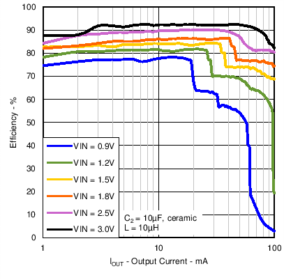 Figure 2. Efficiency vs Output current
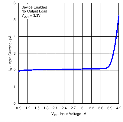 Figure 4. Input Current vs Input Voltage
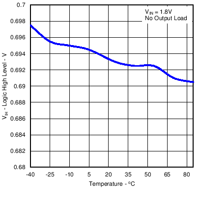 Figure 6. VIH vs Temperature
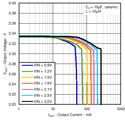 Figure 8. Output Voltage vs Output Current
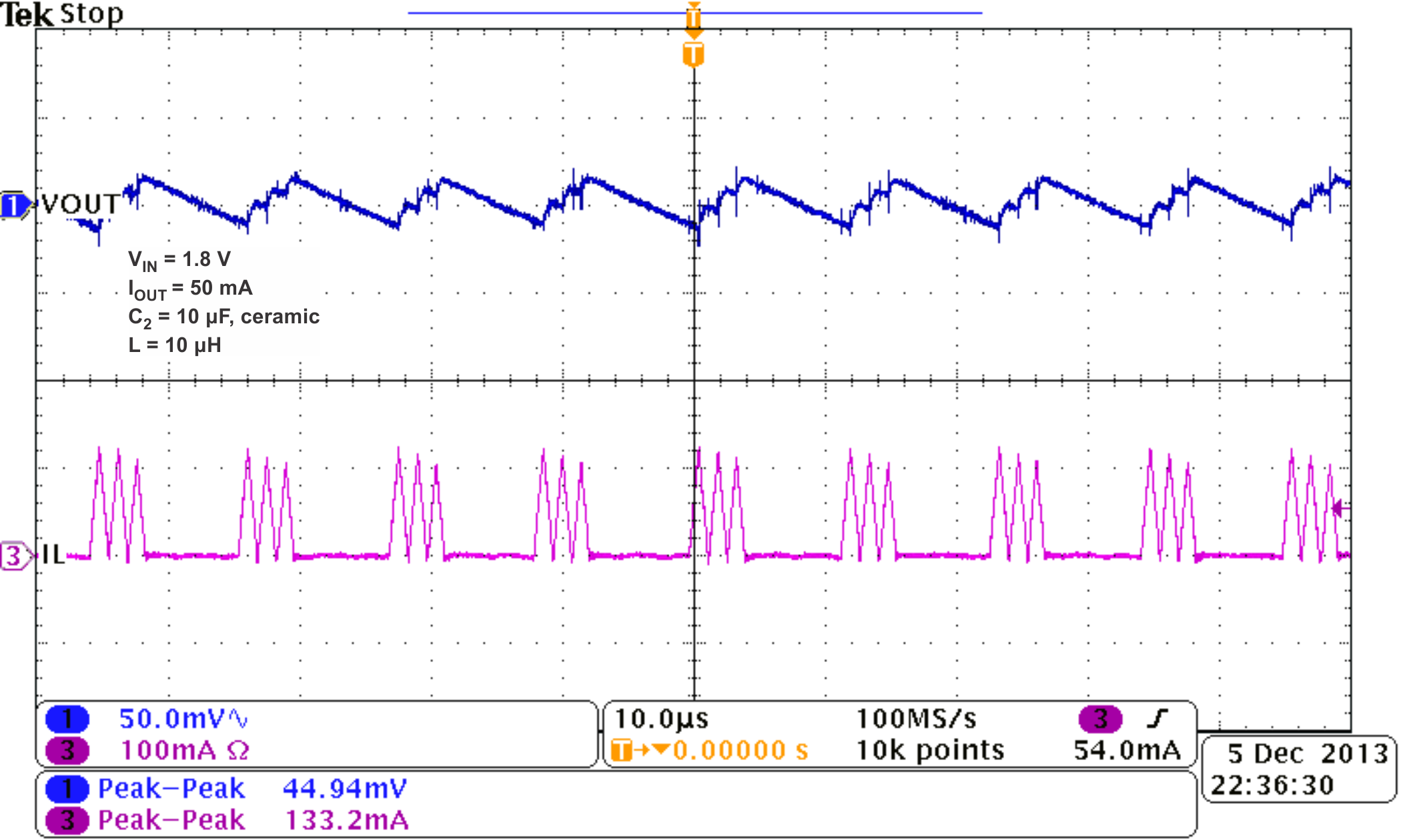
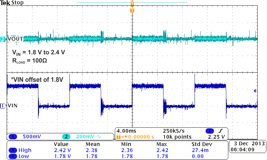 Figure 12. Line Transient Response
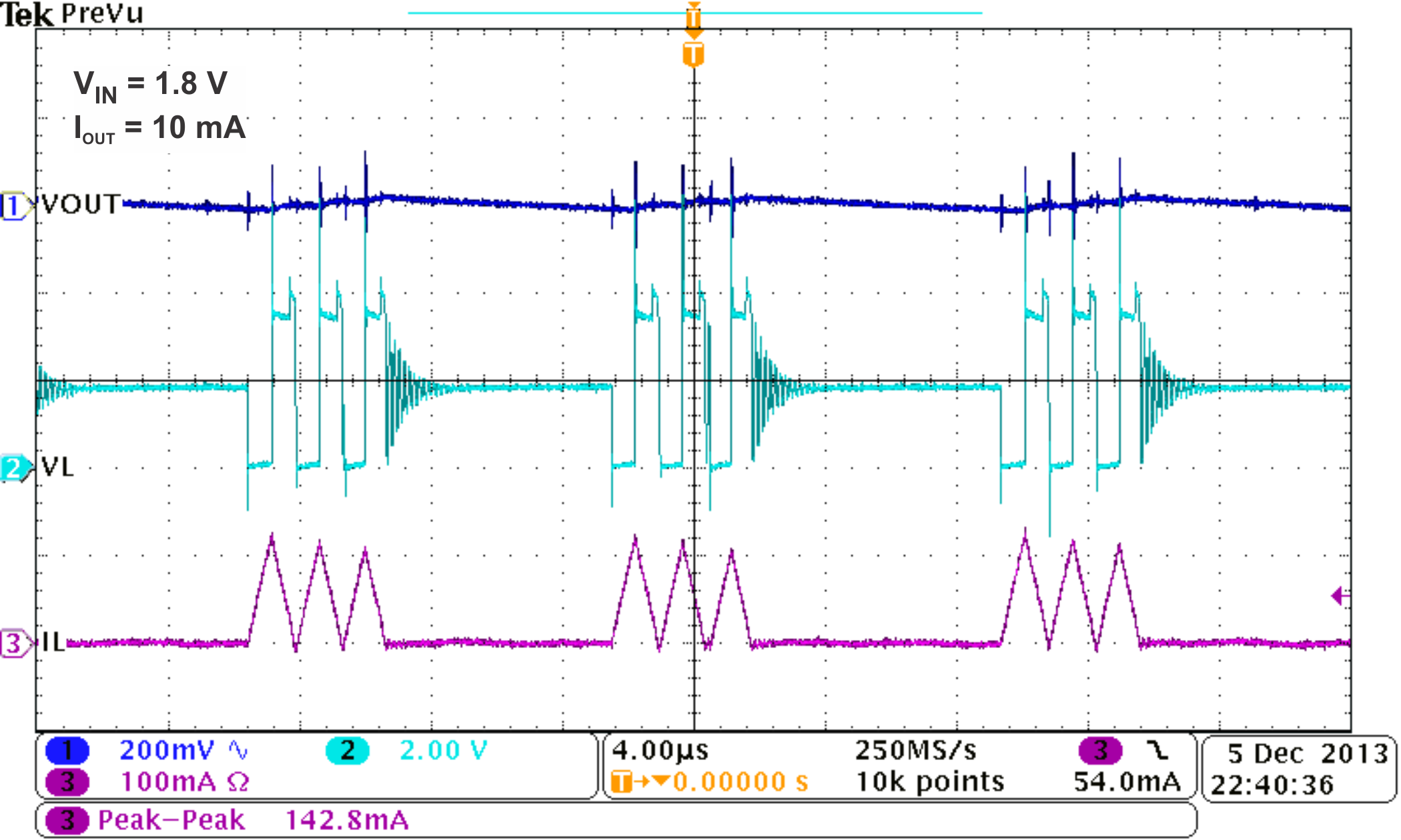 Figure 14. Switching Waveform, Discontinuous Mode