SLVS372C June 2001 – October 2015 TPS60240 , TPS60241 , TPS60242 , TPS60243
PRODUCTION DATA.
- 1 Features
- 2 Applications
- 3 Description
- 4 Revision History
- 5 Pin Configuration and Functions
- 6 Specifications
- 7 Detailed Description
- 8 Application and Implementation
- 9 Power Supply Recommendations
- 10Layout
- 11Device and Documentation Support
- 12Mechanical, Packaging, and Orderable Information
封裝選項(xiàng)
請(qǐng)參考 PDF 數(shù)據(jù)表獲取器件具體的封裝圖。
機(jī)械數(shù)據(jù) (封裝 | 引腳)
- DGK|8
散熱焊盤機(jī)械數(shù)據(jù) (封裝 | 引腳)
訂購(gòu)信息
8 Application and Implementation
NOTE
Information in the following applications sections is not part of the TI component specification, and TI does not warrant its accuracy or completeness. TI’s customers are responsible for determining suitability of components for their purposes. Customers should validate and test their design implementation to confirm system functionality.
8.1 Application Information
The TPS6024x is a switched capacitor voltage converter for VCO and PLL applications providing low noise conversion and tight tolerances. It supports regulated output voltages of 2.7 V, 3 V and 3.3 V from a 1.8-V to 5.5-V input voltage range. The TPS60241 generates 5-V output voltage from an 2.7-V to 5.5-V input voltage range.
8.2 Typical Applications
8.2.1 5-V Low-Noise VCO Supply from 3.3-V Input
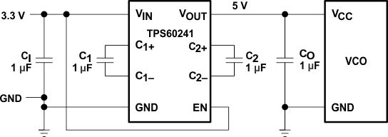 Figure 4. 5-V Low-Noise VCO Supply from 3.3-V Input
8.2.1.1 Design Requirements
The complete charge pump circuitry requires no inductors and only four small ceramic capacitors.
8.2.1.2 Detailed Design Procedure
8.2.1.2.1 Output Voltage Ripple
The output voltage ripple depends on the capacitors used. Table 1 shows the dependence between output voltage ripple and capacitor selection.
Table 1. Output Voltage Ripple and Capacitor Selection(1)
| CI | CO | C1 | C2 | OUTPUT VOLTAGE RIPPLE [µVrms] |
|---|---|---|---|---|
| 1 µF | 1 µF | 1 µF | 1 µF | 288 |
| 2.2 µF | 2.2 µF | 1 µF | 1 µF | 212 |
| 4.7 µF | 4.7 µF | 1 µF | 1 µF | 183 |
| 4.7 µF | 1 µF | 1 µF | 1 µF | 272 |
| 1 µF | 4.7 µF | 1 µF | 1 µF | 185 |
For the best output ripple performance, low-ESR ceramic capacitors are recommended (see Table 2).
Table 2. Recommended Capacitors
| PART | MANUFACTURER | PART NUMBER | VALUE | TOLERANCE | DIELECTRIC MATERIAL | PACKAGE | RATED VOLTAGE |
|---|---|---|---|---|---|---|---|
| CI | Taiyo Yuden | LMK212BJ105KG–T | 1 µF | 10% | X7R | 0805 | 10 |
| TDK | C2012X5R0J475K | 4.7 µF | 10% | X5R | 0805 | 6.3 | |
| CO | Taiyo Yuden | LMK212BJ105KG–T | 1 µF | 10% | X7R | 0805 | 10 |
| TDK | C2012X5R0J475K | 4.7 µF | 10% | X5R | 0805 | 6.3 | |
| C1, C2 | Taiyo Yuden | LMK212BJ105KG–T | 1 µF | 10% | X7R | 0805 | 10 |
| CF | Taiyo Yuden | LMK212BJ105KG–T | 1 µF | 10% | X7R | 0805 | 10 |
8.2.1.3 Application Curves
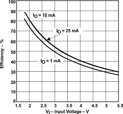 Figure 5. TPS60240
 Efficiency vs Input Voltage
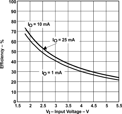 Figure 7. TPS60242
 Efficiency vs Input Voltage
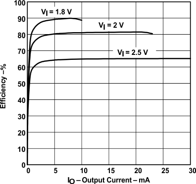 Figure 9. TPS60240
 Efficiency vs Output Voltage
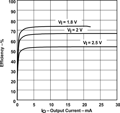 Figure 11. TPS60242
 Efficiency vs Output Voltage
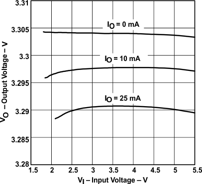 Figure 13. TPS60240
 Output Voltage vs Input Voltage
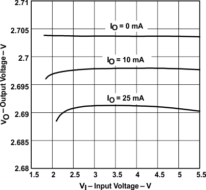 Figure 15. TPS60242
 Output Voltage vs Input Voltage
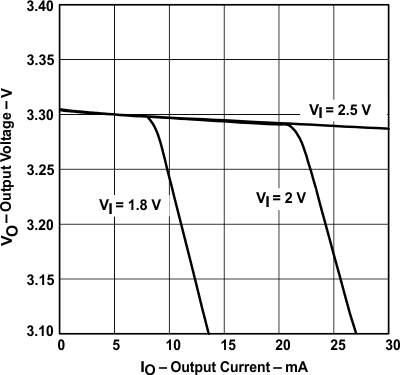 Figure 17. TPS60240
 Output Voltage vs Output Current
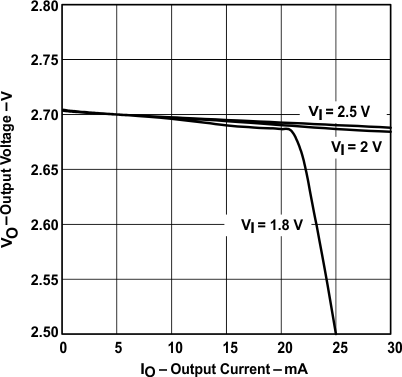 Figure 19. TPS60242
 Output Voltage vs Output Current
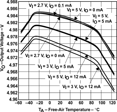 Figure 21. TPS60241
 Output Voltage vs Free-Air Temperature
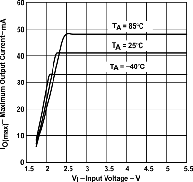 Figure 23. TPS60240
 Maximum Output Current vs Input Voltage
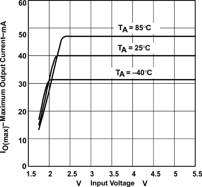 Figure 25. TPS60242
 Maximum Output Current vs Input Voltage
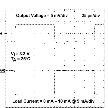 Figure 27. Load Transient Response
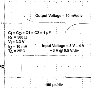 Figure 29. Line Transient Response
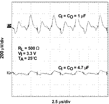
| NOTE: Scope triggered by voltage at flying capacitors, noise removed by averaging function and bandwidth limit 20 MHz. |
Output Voltage Ripple vs Time
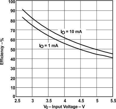 Figure 6. TPS60241
 Efficiency vs Input Voltage
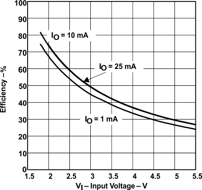 Figure 8. TPS60243
 Efficiency vs Input Voltage
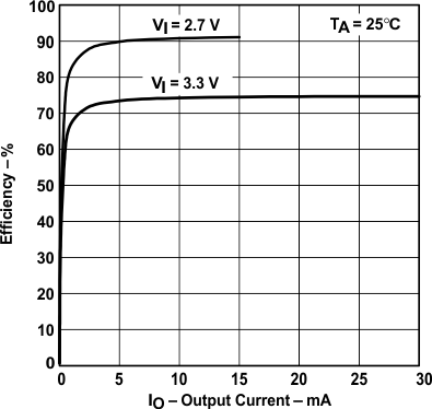 Figure 10. TPS60241
 Efficiency vs Output Voltage
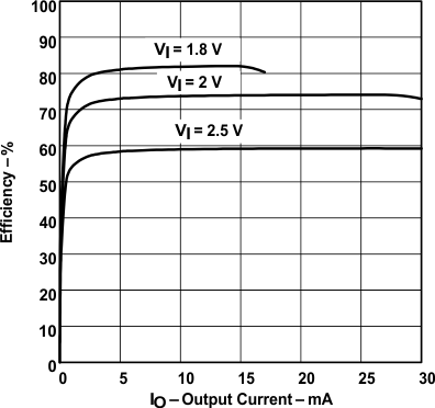 Figure 12. TPS60243
 Efficiency vs Output Voltage
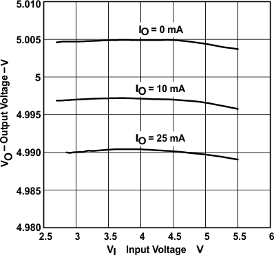 Figure 14. TPS60241
 Output Voltage vs Input Voltage
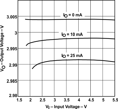 Figure 16. TPS60243
 Output Voltage vs Input Voltage
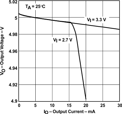 Figure 18. TPS60241
 Output Voltage vs Output Current
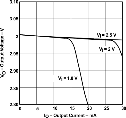 Figure 20. TPS60243
 Output Voltage vs Output Current
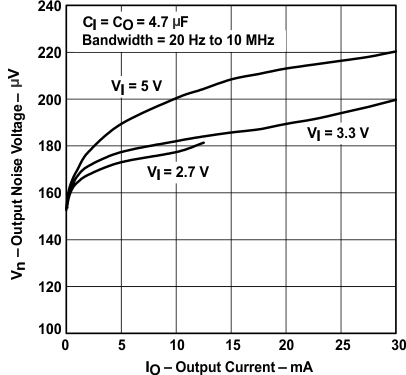 Figure 22. TPS60241
 Output Noise Voltage vs Output Current
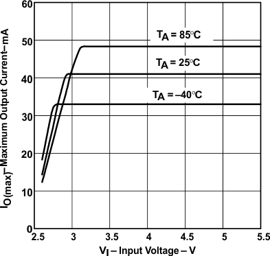 Figure 24. TPS60241
 Maximum Output Current vs Input Voltage
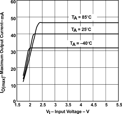 Figure 26. TPS60243
 Maximum Output Current vs Input Voltage
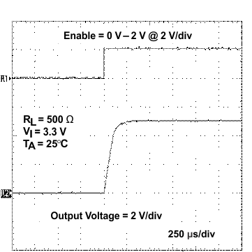 Figure 28. Start-Up Timing
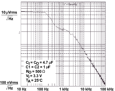 Figure 30. TPS60241
 Noise Voltage Spectrum
8.2.2 2-V to 3.3-V Low-Noise Converter
Standard application as a low noise boost converter. The device generates a regulated output voltage of 3.3 V from a 2-V supply with only 4 external 1-µF ceramic capacitors.
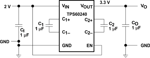 Figure 32. 2-V to 3.3-V Low-Noise Converter