SLAS549D September 2008 – November 2014 TLV320AIC3254
PRODUCTION DATA.
- 1 Features
- 2 Applications
- 3 Description
- 4 Simplified Block Diagram
- 5 Revision History
- 6 Device Comparison Table
- 7 Pin Configuration and Functions
-
8 Specifications
- 8.1 Absolute Maximum Ratings
- 8.2 Handling Ratings
- 8.3 Recommended Operating Conditions
- 8.4 Thermal Information
- 8.5 Electrical Characteristics, ADC
- 8.6 Electrical Characteristics, Bypass Outputs
- 8.7 Electrical Characteristics, Microphone Interface
- 8.8 Electrical Characteristics, Audio DAC Outputs
- 8.9 Electrical Characteristics, LDO
- 8.10 Electrical Characteristics, Misc.
- 8.11 Electrical Characteristics, Logic Levels
- 8.12 I2S LJF and RJF Timing in Master Mode (see )
- 8.13 I2S LJF and RJF Timing in Slave Mode (see )
- 8.14 DSP Timing in Master Mode (see )
- 8.15 DSP Timing in Slave Mode (see )
- 8.16 Digital Microphone PDM Timing (see )
- 8.17 I2C Interface Timing
- 8.18 SPI Interface Timing (See )
- 8.19 Typical Characteristics
- 8.20 Typical Characteristics, FFT
- 9 Parameter Measurement Information
-
10Detailed Description
- 10.1 Overview
- 10.2 Functional Block Diagram
- 10.3 Feature Description
- 10.4 Device Functional Modes
- 10.5 Software
- 10.6 Register Map
- 11Applications and Implementation
- 12Power Supply Recommendations
- 13Layout
- 14Device and Documentation Support
- 15Mechanical, Packaging, and Orderable Information
8 Specifications
8.1 Absolute Maximum Ratings
over operating free-air temperature range (unless otherwise noted) (1)| MIN | MAX | UNIT | ||
|---|---|---|---|---|
| Input voltage | AVDD to AVSS | –0.3 | 2.2 | V |
| DVDD to DVSS | –0.3 | 2.2 | V | |
| IOVDD to IOVSS | –0.3 | 3.9 | V | |
| LDOIN to AVSS | –0.3 | 3.9 | V | |
| Digital Input voltage to ground | –0.3 | IOVDD + 0.3 | V | |
| Analog input voltage to ground | –0.3 | AVDD + 0.3 | V | |
| Operating temperature range | –40 | 85 | °C | |
| Junction temperature (TJ Max) | 105 | °C | ||
(1) Stresses beyond those listed under “absolute maximum ratings” may cause permanent damage to the device. These are stress ratings only, and functional operation of the device at these or any other conditions beyond those indicated under “recommended operating conditions” is not implied. Exposure to absolute-maximum-rated conditions for extended periods may affect device reliability.
8.2 Handling Ratings
| MIN | MAX | UNIT | ||||
|---|---|---|---|---|---|---|
| Tstg | Storage temperature range | –55 | 125 | °C | ||
| V(ESD) | Electrostatic discharge | Human body model (HBM), per ANSI/ESDA/JEDEC JS-001, all pins(1) | –2 | 2 | kV | |
| Charged device model (CDM), per JEDEC specification JESD22-C101, all pins(2) | –750 | 750 | V | |||
(1) JEDEC document JEP155 states that 500-V HBM allows safe manufacturing with a standard ESD control process.
(2) JEDEC document JEP157 states that 250-V CDM allows safe manufacturing with a standard ESD control process.
8.3 Recommended Operating Conditions
| MIN | NOM | MAX | UNIT | ||||
|---|---|---|---|---|---|---|---|
| LDOIN | Power Supply Voltage Range | Referenced to AVSS(1) | 1.9 | 3.6 | V | ||
| AVDD | 1.5 | 1.8 | 1.95 | ||||
| IOVDD | Referenced to IOVSS(1) | 1.1 | 3.6 | ||||
| DVDD(2) | Referenced to DVSS(1) | 1.26 | 1.8 | 1.95 | |||
| PLL Input Frequency | Clock divider uses fractional divide (D > 0), P = 1, DVDD ≥ 1.65V (Refer to the table in SLAA408, Maximum TLV320AIC3254 Clock Frequencies) |
10 | 20 | MHz | |||
| Clock divider uses integer divide (D = 0), P = 1, DVDD ≥ 1.65V (Refer to the table in SLAA408, Maximum TLV320AIC3254 Clock Frequencies) |
0.512 | 20 | MHz | ||||
| MCLK | Master Clock Frequency | MCLK; Master Clock Frequency; DVDD ≥ 1.65V | 50 | MHz | |||
| MCLK; Master Clock Frequency; DVDD ≥ 1.26V | 25 | ||||||
| SCL | SCL Clock Frequency | 400 | kHz | ||||
| Audio input max ac signal swing
(IN1_L, IN1_R, IN2_L, IN2_R, IN3_L, IN3_R) |
CM = 0.75 V | 0 | 0.530 | 0.75 or AVDD-0.75(3) |
Vpeak | ||
| CM = 0.9 V | 0 | 0.707 | 0.9 or AVDD-0.9(3) |
Vpeak | |||
| LOL, LOR | Stereo line output load resistance | 0.6 | 10 | kΩ | |||
| HPL, HPR | Stereo headphone output load resistance | Single-ended configuration | 14.4 | 16 | Ω | ||
| Headphone output load resistance | Differential configuration | 24.4 | 32 | Ω | |||
| CLout | Digital output load capacitance | 10 | pF | ||||
| TOPR | Operating Temperature Range | –40 | 85 | °C | |||
(1) All grounds on board are tied together to prevent voltage differences of more than 0.2V maximum for any combination of ground signals.
(2) At DVDD values lower than 1.65V, the PLL does not function. Refer to the Maximum TLV320AIC3254 Clock Frequencies table in the TLV320AIC3254 Application Reference Guide(SLAA408) for details on maximum clock frequencies.
(3) Whichever is smaller.
8.4 Thermal Information
| THERMAL METRIC(1) | TLV320AIC3254 | UNIT | |
|---|---|---|---|
| RHB (32 PINS) | |||
| RθJA | Junction-to-ambient thermal resistance | 31.4 | °C/W |
| RθJCtop | Junction-to-case (top) thermal resistance | 21.4 | |
| RθJB | Junction-to-board thermal resistance | 5.4 | |
| ψJT | Junction-to-top characterization parameter | 0.2 | |
| ψJB | Junction-to-board characterization parameter | 5.4 | |
| RθJCbot | Junction-to-case (bottom) thermal resistance | 0.9 | |
(1) For more information about traditional and new thermal metrics, see the IC Package Thermal Metrics application report, SPRA953.
8.5 Electrical Characteristics, ADC
At 25°C, AVDD, DVDD, IOVDD = 1.8V, LDOIN = 3.3V, AVDD and DVDD LDO disabled, fs (Audio) = 48kHz, Cref = 10µF on REF pin, PLL disabled unless otherwise noted.| PARAMETER | TEST CONDITIONS | MIN | TYP | MAX | UNIT | |
|---|---|---|---|---|---|---|
| AUDIO ADC | ||||||
| Input signal level (0dB) | Single-ended, CM = 0.9V | 0.5 | VRMS | |||
| Device Setup | 1kHz sine wave input , Single-ended Configuration IN1_R to Right ADC and IN1_L to Left ADC, Rin = 20K, fs = 48kHz, AOSR = 128, MCLK = 256 x fs, PLL Disabled; AGC = OFF, Channel Gain = 0dB, Processing Block = PRB_R1, Power Tune = PTM_R4 |
|||||
| SNR | Signal-to-noise ratio, A-weighted(1)(2) | Inputs ac-shorted to ground | 80 | 93 | dB | |
| IN2_R, IN3_R routed to Right ADC and ac-shorted to ground IN2_L, IN3_L routed to Left ADC and ac-shorted to ground |
93 | |||||
| DR | Dynamic range A-weighted(1)(2) | –60dB full-scale, 1-kHz input signal | 92 | dB | ||
| THD+N | Total Harmonic Distortion plus Noise | –3 dB full-scale, 1-kHz input signal | –85 | –70 | dB | |
| IN2_R, IN3_R routed to Right ADC IN2_L, IN3_L routed to Left ADC –3dB full-scale, 1-kHz input signal |
–85 | |||||
| AUDIO ADC | ||||||
| Input signal level (0dB) | Single-ended, CM = 0.75V, AVDD = 1.5V | 0.375 | VRMS | |||
| Device Setup | 1kHz sine wave input, Single-ended Configuration IN1_R, IN2_R, IN3_R routed to Right ADC IN1_L, IN2_L, IN3_L routed to Left ADC Rin = 20kΩ, fs = 48kHz, AOSR = 128, MCLK = 256 x fs, PLL Disabled, AGC = OFF, Channel Gain = 0dB, Processing Block = PRB_R1 Power Tune = PTM_R4 |
|||||
| SNR | Signal-to-noise ratio, A-weighted (1)(2) | Inputs ac-shorted to ground | 91 | dB | ||
| DR | Dynamic range A-weighted(1)(2) | –60dB full-scale, 1-kHz input signal | 90 | dB | ||
| THD+N | Total Harmonic Distortion plus Noise | –3dB full-scale, 1-kHz input signal | –80 | dB | ||
| AUDIO ADC | ||||||
| Input signal level (0dB) | Differential Input, CM = 0.9V | 10 | mV | |||
| Device Setup | 1kHz sine wave input, Differential configuration IN1_L and IN1_R routed to Right ADC IN2_L and IN2_R routed to Left ADC Rin = 10K, fs = 48kHz, AOSR = 128 MCLK = 256* fs PLL Disabled AGC = OFF, Channel Gain = 40dB Processing Block = PRB_R1, Power Tune = PTM_R4 |
|||||
| ICN | Idle-Channel Noise, A-weighted(1)(2) | Inputs ac-shorted to ground, input referred noise | 2 | μVRMS | ||
| AUDIO ADC | ||||||
| Gain Error | 1kHz sine wave input , Single-ended configuration Rin = 20kΩ fs = 48kHz, AOSR = 128, MCLK = 256 x fs, PLL Disabled AGC = OFF, Channel Gain = 0dB Processing Block = PRB_R1, Power Tune = PTM_R4, CM = 0.9V |
–0.05 | dB | |||
| Input Channel Separation | 1kHz sine wave input at -3dBFS Single-ended configuration IN1_L routed to Left ADC IN1_R routed to Right ADC, Rin = 20kΩ AGC = OFF, AOSR = 128, Channel Gain = 0dB, CM = 0.9V |
108 | dB | |||
| Input Pin Crosstalk | 1kHz sine wave input at –3dBFS on IN2_L, IN2_L internally not routed. IN1_L routed to Left ADC ac-coupled to ground |
115 | dB | |||
| 1kHz sine wave input at –3dBFS on IN2_R, IN2_R internally not routed. IN1_R routed to Right ADC ac-coupled to ground |
||||||
| Single-ended configuration Rin = 20kΩ, AOSR = 128 Channel, Gain = 0dB, CM = 0.9V |
||||||
| PSRR | 217Hz, 100mVpp signal on AVDD, Single-ended configuration, Rin = 20kΩ, Channel Gain = 0dB; CM = 0.9V |
55 | dB | |||
| ADC programmable gain amplifier gain | Single-Ended, Rin = 10kΩ, PGA gain set to 0dB | 0 | dB | |||
| Single-Ended, Rin = 10kΩ, PGA gain set to 47.5dB | 47.5 | dB | ||||
| Single-Ended, Rin = 20kΩ, PGA gain set to 0dB | –6 | dB | ||||
| Single-Ended, Rin = 20kΩ, PGA gain set to 47.5dB | 41.5 | dB | ||||
| Single-Ended, Rin = 40kΩ, PGA gain set to 0dB | –12 | dB | ||||
| Single-Ended, Rin = 40kΩ, PGA gain set to 47.5dB | 35.5 | dB | ||||
| ADC programmable gain amplifier step size | 1-kHz tone | 0.5 | dB | |||
(1) Ratio of output level with 1kHz full-scale sine wave input, to the output level with the inputs short circuited, measured A-weighted over a 20Hz to 20kHz bandwidth using an audio analyzer.
(2) All performance measured with 20kHz low-pass filter and, where noted, A-weighted filter. Failure to use such a filter may result in higher THD+N and lower SNR and dynamic range readings than shown in the Electrical Characteristics. The low-pass filter removes out-of-band noise, which, although not audible, may affect dynamic specification values.
8.6 Electrical Characteristics, Bypass Outputs
At 25°C, AVDD, DVDD, IOVDD = 1.8V, LDOIN = 3.3V, AVDD and DVDD LDO disabled, fs (Audio) = 48kHz, Cref = 10µF on REF pin, PLL disabled unless otherwise noted.| PARAMETER | TEST CONDITIONS | MIN | TYP | MAX | UNIT | |
|---|---|---|---|---|---|---|
| ANALOG BYPASS TO HEADPHONE AMPLIFIER, DIRECT MODE | ||||||
| Device Setup | Load = 16Ω (single-ended), 50pF; Input and Output CM = 0.9V; Headphone Output on LDOIN Supply; IN1_L routed to HPL and IN1_R routed to HPR; Channel Gain = 0dB |
|||||
| Gain Error | –0.8 | dB | ||||
| Noise, A-weighted(1) | Idle Channel, IN1_L and IN1_R ac-shorted to ground | 3 | μVRMS | |||
| THD | Total Harmonic Distortion | 446mVrms, 1kHz input signal | –89 | dB | ||
| ANALOG BYPASS TO LINE-OUT AMPLIFIER, PGA MODE | ||||||
| Device Setup | Load = 10kΩ (single-ended), 56pF; Input and Output CM = 0.9V; LINE Output on LDOIN Supply; IN1_L routed to ADCPGA_L and IN1_R routed to ADCPGA_R; Rin = 20kΩ ADCPGA_L routed to LOL and ADCPGA_R routed to LOR; Channel Gain = 0dB |
|||||
| Gain Error | 0.6 | dB | ||||
| Noise, A-weighted(1) | Idle Channel, IN1_L and IN1_R ac-shorted to ground |
7 | μVRMS | |||
| Channel Gain = 40dB, Input Signal (0dB) = 5mVrms Inputs ac-shorted to ground, Input Referred |
3.4 | μVRMS | ||||
(1) All performance measured with 20kHz low-pass filter and, where noted, A-weighted filter. Testing without such a filter may result in higher THD+N and lower SNR and dynamic range readings than shown in the Electrical Characteristics. The low-pass filter removes out-of-band noise, which, although not audible, may affect dynamic specification values.
8.7 Electrical Characteristics, Microphone Interface
At 25°C, AVDD, DVDD, IOVDD = 1.8V, LDOIN = 3.3V, AVDD and DVDD LDO disabled, fs (Audio) = 48kHz, Cref = 10µF on REF pin, PLL disabled unless otherwise noted.| PARAMETER | TEST CONDITIONS | MIN | TYP | MAX | UNIT | |
|---|---|---|---|---|---|---|
| MICROPHONE BIAS | ||||||
| Bias voltage | Bias voltage CM = 0.9V, LDOIN = 3.3V | |||||
| Micbias Mode 0, Connect to AVDD or LDOIN | 1.25 | V | ||||
| Micbias Mode 1, Connect to LDOIN | 1.7 | V | ||||
| Micbias Mode 2, Connect to LDOIN | 2.5 | V | ||||
| Micbias Mode 3, Connect to AVDD | AVDD | V | ||||
| Micbias Mode 3, Connect to LDOIN | LDOIN | V | ||||
| CM = 0.75V, LDOIN = 3.3V | ||||||
| Micbias Mode 0, Connect to AVDD or LDOIN | 1.04 | V | ||||
| Micbias Mode 1, Connect to AVDD or LDOIN | 1.425 | V | ||||
| Micbias Mode 2, Connect to LDOIN | 2.075 | V | ||||
| Micbias Mode 3, Connect to AVDD | AVDD | V | ||||
| Micbias Mode 3, Connect to LDOIN | LDOIN | V | ||||
| Output Noise | CM = 0.9V, Micbias Mode 2, A-weighted, 20Hz to 20kHz bandwidth, Current load = 0mA. |
10 | μVRMS | |||
| Current Sourcing | Micbias Mode 2, Connect to LDOIN | 3 | mA | |||
| Inline Resistance | Micbias Mode 3, Connect to AVDD | 140 | Ω | |||
| Micbias Mode 3, Connect to LDOIN | 87 | |||||
8.8 Electrical Characteristics, Audio DAC Outputs
At 25°C, AVDD, DVDD, IOVDD = 1.8V, LDOIN = 3.3V, AVDD and DVDD LDO disabled, fs (Audio) = 48kHz, Cref = 10µF on REF pin, PLL disabled unless otherwise noted.| PARAMETER | TEST CONDITIONS | MIN | TYP | MAX | UNIT | |
|---|---|---|---|---|---|---|
| AUDIO DAC – STEREO SINGLE-ENDED LINE OUTPUT | ||||||
| Device Setup | Load = 10kΩ (single-ended), 56pF Line Output on AVDD Supply Input and Output CM = 0.9V DOSR = 128, MCLK = 256 x fs, Channel Gain = 0dB, word length = 16 bits, Processing Block = PRB_P1, Power Tune = PTM_P3 |
|||||
| Full scale output voltage (0dB) | 0.5 | VRMS | ||||
| SNR | Signal-to-noise ratio A-weighted(1)(2) | All zeros fed to DAC input | 87 | 100 | dB | |
| DR | Dynamic range, A-weighted(1)(2) | –60dB 1kHz input full-scale signal, Word length = 20 bits | 100 | dB | ||
| THD+N | Total Harmonic Distortion plus Noise | –3dB full-scale, 1kHz input signal | –83 | –70 | dB | |
| DAC Gain Error | 0 dB, 1kHz input full scale signal | 0.3 | dB | |||
| DAC Mute Attenuation | Mute | 119 | dB | |||
| DAC channel separation | –1 dB, 1kHz signal, between left and right HP out | 113 | dB | |||
| DAC PSRR | 100mVpp, 1kHz signal applied to AVDD | 73 | dB | |||
| 100mVpp, 217Hz signal applied to AVDD | 77 | dB | ||||
| AUDIO DAC – STEREO SINGLE-ENDED LINE OUTPUT | ||||||
| Device Setup | Load = 10kΩ (single-ended), 56pF Line Output on AVDD Supply Input and Output CM = 0.75V; AVDD = 1.5V DOSR = 128 MCLK = 256 * fs Channel Gain = –2dB word length = 20 bits Processing Block = PRB_P1 Power Tune = PTM_P4 |
|||||
| Full scale output voltage (0dB) | 0.375 | VRMS | ||||
| SNR | Signal-to-noise ratio, A-weighted(1)(2) | All zeros fed to DAC input | 99 | dB | ||
| DR | Dynamic range, A-weighted(1)(2) | –60dB 1 kHz input full-scale signal | 97 | dB | ||
| THD+N | Total Harmonic Distortion plus Noise | –1 dB full-scale, 1-kHz input signal | –85 | dB | ||
| AUDIO DAC – STEREO SINGLE-ENDED HEADPHONE OUTPUT | ||||||
| Device Setup | Load = 16Ω (single-ended), 50pF Headphone Output on AVDD Supply, Input and Output CM = 0.9V, DOSR = 128, MCLK = 256 * fs, Channel Gain = 0dB word length = 16 bits; Processing Block = PRB_P1 Power Tune = PTM_P3 |
|||||
| Full scale output voltage (0dB) | 0.5 | VRMS | ||||
| SNR | Signal-to-noise ratio, A-weighted(1)(2) | All zeros fed to DAC input | 87 | 100 | dB | |
| DR | Dynamic range, A-weighted(1)(2) | –60dB 1kHz input full-scale signal, Word Length = 20 bits, Power Tune = PTM_P4 | 99 | dB | ||
| THD+N | Total Harmonic Distortion plus Noise | –3dB full-scale, 1kHz input signal | –83 | –70 | dB | |
| DAC Gain Error | 0dB, 1kHz input full scale signal | –0.3 | dB | |||
| DAC Mute Attenuation | Mute | 122 | dB | |||
| DAC channel separation | –1dB, 1kHz signal, between left and right HP out | 110 | dB | |||
| DAC PSRR | 100mVpp, 1kHz signal applied to AVDD | 73 | dB | |||
| 100mVpp, 217Hz signal applied to AVDD | 78 | dB | ||||
| Power Delivered | RL = 16Ω, Output Stage on AVDD = 1.8V THDN < 1%, Input CM = 0.9V, Output CM = 0.9V |
15 | mW | |||
| RL = 16Ω Output Stage on LDOIN = 3.3V, THDN < 1% Input CM = 0.9V, Output CM = 1.65V |
64 | |||||
| AUDIO DAC – STEREO SINGLE-ENDED HEADPHONE OUTPUT | ||||||
| Device Setup | Load = 16Ω (single-ended), 50pF, Headphone Output on AVDD Supply, Input and Output CM = 0.75V; AVDD = 1.5V, DOSR = 128, MCLK = 256 * fs, Channel Gain = –2dB, word length = 20-bits; Processing Block = PRB_P1, Power Tune = PTM_P4 |
|||||
| Full scale output voltage (0dB) | 0.375 | VRMS | ||||
| SNR | Signal-to-noise ratio, A-weighted(1)(2) | All zeros fed to DAC input | 99 | dB | ||
| DR | Dynamic range, A-weighted(1)(2) | -60dB 1kHz input full-scale signal | 98 | dB | ||
| THD+N | Total Harmonic Distortion plus Noise | –1dB full-scale, 1kHz input signal | –83 | dB | ||
| AUDIO DAC – MONO DIFFERENTIAL HEADPHONE OUTPUT | ||||||
| Device Setup | Load = 32Ω (differential), 50pF, Headphone Output on LDOIN Supply Input CM = 0.75V, Output CM = 1.5V, AVDD = 1.8V, LDOIN = 3.0V, DOSR = 128 MCLK = 256 * fs, Channel (headphone driver) Gain = 5dB for full scale output signal, word length = 16 bits, Processing Block = PRB_P1, Power Tune = PTM_P3 |
|||||
| Full scale output voltage (0dB) | 1778 | mVRMS | ||||
| SNR | Signal-to-noise ratio, A-weighted(1)(2) | All zeros fed to DAC input | 98 | dB | ||
| DR | Dynamic range, A-weighted(1)(2) | –60dB 1kHz input full-scale signal | 96 | dB | ||
| THD | Total Harmonic Distortion | –3dB full-scale, 1kHz input signal | –82 | dB | ||
| Power Delivered | RL = 32Ω, Output Stage on LDOIN = 3.3V, THDN < 1%, Input CM = 0.9V, Output CM = 1.65V |
136 | mW | |||
| RL = 32Ω Output Stage on LDOIN = 3.0V, THDN < 1% Input CM = 0.9V, Output CM = 1.5V |
114 | mW | ||||
(1) Ratio of output level with 1kHz full-scale sine wave input, to the output level with the inputs short circuited, measured A-weighted over a 20Hz to 20kHz bandwidth using an audio analyzer.
(2) All performance measured with 20kHz low-pass filter and, where noted, A-weighted filter. Testing without such a filter may result in higher THD+N and lower SNR and dynamic range readings than shown in the Electrical Characteristics. The low-pass filter removes out-of-band noise, which, although not audible, may affect dynamic specification values
8.9 Electrical Characteristics, LDO
over operating free-air temperature range (unless otherwise noted)| PARAMETER | TEST CONDITIONS | MIN | TYP | MAX | UNIT | |
|---|---|---|---|---|---|---|
| LOW DROPOUT REGULATOR (AVdd) | ||||||
| Output Voltage | LDOMode = 1, LDOIN > 1.95V | 1.67 | V | |||
| LDOMode = 0, LDOIN > 2.0V | 1.72 | |||||
| LDOMode = 2, LDOIN > 2.05V | 1.77 | |||||
| Output Voltage Accuracy | ±2% | |||||
| Load Regulation | Load current range 0 to 50mA | 15 | mV | |||
| Line Regulation | Input Supply Range 1.9V to 3.6V | 5 | mV | |||
| Decoupling Capacitor | 1 | μF | ||||
| Bias Current | 60 | μA | ||||
| LOW DROPOUT REGULATOR (DVdd) | ||||||
| Output Voltage | LDOMode = 1, LDOIN > 1.95V | 1.67 | V | |||
| LDOMode = 0, LDOIN > 2.0V | 1.72 | |||||
| LDOMode = 2, LDOIN > 2.05V | 1.77 | |||||
| Output Voltage Accuracy | ±%2 | |||||
| Load Regulation | Load current range 0 to 50mA | 15 | mV | |||
| Line Regulation | Input Supply Range 1.9V to 3.6V | 5 | mV | |||
| Decoupling Capacitor | 1 | μF | ||||
| Bias Current | 60 | μA | ||||
8.10 Electrical Characteristics, Misc.
At 25°C, AVDD, DVDD, IOVDD = 1.8V, LDOIN = 3.3V, AVDD and DVDD LDO disabled, fs (Audio) = 48kHz, Cref = 10µF on REF pin, PLL disabled unless otherwise noted.| PARAMETER | TEST CONDITIONS | MIN | TYP | MAX | UNIT | |
|---|---|---|---|---|---|---|
| REFERENCE | ||||||
| Reference Voltage Settings | CMMode = 0 (0.9V) | 0.9 | V | |||
| CMMode = 1 (0.75V) | 0.75 | |||||
| Reference Noise | CM = 0.9V, A-weighted, 20Hz to 20kHz bandwidth, Cref = 10μF | 1 | μVRfcMS | |||
| Decoupling Capacitor | 1 | 10 | μF | |||
| miniDSP(1) | ||||||
| Maximum miniDSP clock frequency - ADC | DVDD = 1.65V | 55.3 | MHz | |||
| Maximum miniDSP clock frequency - DAC | DVDD = 1.65V | 55.3 | MHz | |||
| Shutdown Current | ||||||
| Device Setup | Coarse AVDD supply turned off, LDO_select held at ground, No external digital input is toggled | |||||
| I(DVDD) | 0.9 | μA | ||||
| I(AVDD) | <0.9 | μA | ||||
| I(LDOIN) | <0.9 | μA | ||||
| I(IOVDD) | 13 | nA | ||||
(1) miniDSP clock speed is specified by design and not tested in production.
8.11 Electrical Characteristics, Logic Levels(1)
At 25°C, AVDD, DVDD, IOVDD = 1.8V| PARAMETER | TEST CONDITIONS | MIN | TYP | MAX | UNIT | |
|---|---|---|---|---|---|---|
| LOGIC FAMILY | CMOS | |||||
| VIH | Logic Level | IIH = 5 μA, IOVDD > 1.6V | 0.7 × IOVDD | V | ||
| IIH = 5μA, 1.2V ≤ IOVDD < 1.6V | 0.9 × IOVDD | V | ||||
| IIH = 5μA, IOVDD < 1.2V | IOVDD | V | ||||
| VIL | IIL = 5 μA, IOVDD > 1.6V | –0.3 | 0.3 × IOVDD | V | ||
| IIL = 5μA, 1.2V ≤ IOVDD < 1.6V | 0.1 × IOVDD | V | ||||
| IIL = 5μA, IOVDD < 1.2V | 0 | V | ||||
| VOH | IOH = 2 TTL loads | 0.8 × IOVDD | V | |||
| VOL | IOL = 2 TTL loads | 0.1 × IOVDD | V | |||
| Capacitive Load | 10 | pF | ||||
(1) Applies to all DI, DO, and DIO pins shown in Pin Configuration and Functions.
8.12 I2S LJF and RJF Timing in Master Mode (see Figure 1)
| IOVDD = 1.8V | IOVDD = 3.3V | UNIT | ||||
|---|---|---|---|---|---|---|
| MIN | MAX | MIN | MAX | |||
| td(WS) | WCLK delay | 30 | 20 | ns | ||
| td(DO-WS) | WCLK to DOUT delay (For LJF Mode only) | 20 | 20 | ns | ||
| td(DO-BCLK) | BCLK to DOUT delay | 22 | 20 | ns | ||
| ts(DI) | DIN setup | 8 | 8 | ns | ||
| th(DI) | DIN hold | 8 | 8 | ns | ||
| tr | Rise time | 24 | 12 | ns | ||
| tf | Fall time | 24 | 12 | ns | ||
All specifications at 25°C, DVdd = 1.8V
Figure 1. I2S LJF and RJF Timing in Master Mode
8.13 I2S LJF and RJF Timing in Slave Mode (see Figure 2)
| IOVDD = 1.8V | IOVDD = 3.3V | UNIT | ||||
|---|---|---|---|---|---|---|
| MIN | MAX | MIN | MAX | |||
| tH(BCLK) | BCLK high period | 35 | 35 | ns | ||
| tL(BCLK) | BCLK low period | 35 | 35 | ns | ||
| ts(WS) | WCLK setup | 8 | 8 | ns | ||
| th(WS) | WCLK hold | 8 | 8 | ns | ||
| td(DO-WS) | WCLK to DOUT delay (For LJF mode only) | 20 | 20 | ns | ||
| td(DO-BCLK) | BCLK to DOUT delay | 22 | 22 | ns | ||
| ts(DI) | DIN setup | 8 | 8 | ns | ||
| th(DI) | DIN hold | 8 | 8 | ns | ||
| tr | Rise time | 4 | 4 | ns | ||
| tf | Fall time | 4 | 4 | ns | ||
 Figure 2. I2S LJF and RJF Timing in Slave Mode
8.14 DSP Timing in Master Mode (see Figure 3)
| IOVDD = 1.8V | IOVDD = 3.3V | UNIT | ||||
|---|---|---|---|---|---|---|
| MIN | MAX | MIN | MAX | |||
| td(WS) | WCLK delay | 30 | 20 | ns | ||
| td(DO-BCLK) | BCLK to DOUT delay | 22 | 20 | ns | ||
| ts(DI) | DIN setup | 8 | 8 | ns | ||
| th(DI) | DIN hold | 8 | 8 | ns | ||
| tr | Rise time | 24 | 12 | ns | ||
| tf | Fall time | 24 | 12 | ns | ||
All specifications at 25°C, DVdd = 1.8V
Figure 3. DSP Timing in Master Mode
8.15 DSP Timing in Slave Mode (see Figure 4)
| IOVDD = 1.8V | IOVDD = 3.3V | UNIT | ||||
|---|---|---|---|---|---|---|
| MIN | MAX | MIN | MAX | |||
| tH(BCLK) | BCLK high period | 35 | 35 | ns | ||
| tL(BCLK) | BCLK low period | 35 | 35 | ns | ||
| ts(WS) | WCLK setup | 8 | 8 | ns | ||
| th(WS) | WCLK hold | 8 | 8 | ns | ||
| td(DO-BCLK) | BCLK to DOUT delay | 22 | 22 | ns | ||
| ts(DI) | DIN setup | 8 | 8 | ns | ||
| th(DI) | DIN hold | 8 | 8 | ns | ||
| tr | Rise time | 4 | 4 | ns | ||
| tf | Fall time | 4 | 4 | ns | ||
 Figure 4. DSP Timing in Slave Mode
8.16 Digital Microphone PDM Timing (see Figure 5)
Based on design simulation. Not tested in actual silicon.| IOVDD = 1.8V | IOVDD = 3.3V | UNIT | ||||
|---|---|---|---|---|---|---|
| MIN | MAX | MIN | MAX | |||
| ts | DIN setup | 20 | 20 | ns | ||
| th | DIN hold | 5 | 5 | ns | ||
| tr | Rise time | 4 | 4 | ns | ||
| tf | Fall time | 4 | 4 | ns | ||
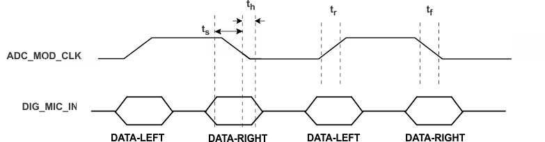 Figure 5. PDM Input Timing
8.17 I2C Interface Timing
| Standard-Mode | Fast-Mode | UNIT | |||||||
|---|---|---|---|---|---|---|---|---|---|
| MIN | TYP | MAX | MIN | TYP | MAX | ||||
| fSCL | SCL clock frequency | 0 | 100 | 0 | 400 | kHz | |||
| tHD;STA | Hold time (repeated) START condition. After this period, the first clock pulse is generated. | 4.0 | 0.8 | μs | |||||
| tLOW | LOW period of the SCL clock | 4.7 | 1.3 | μs | |||||
| tHIGH | HIGH period of the SCL clock | 4.0 | 0.6 | μs | |||||
| tSU;STA | Setup time for a repeated START condition | 4.7 | 0.8 | μs | |||||
| tHD;DAT | Data hold time: For I2C bus devices | 0 | 3.45 | 0 | 0.9 | μs | |||
| tSU;DAT | Data set-up time | 250 | 100 | ns | |||||
| tr | SDA and SCL Rise Time | 1000 | 20+0.1Cb | 300 | ns | ||||
| tf | SDA and SCL Fall Time | 300 | 20+0.1Cb | 300 | ns | ||||
| tSU;STO | Set-up time for STOP condition | 4.0 | 0.8 | μs | |||||
| tBUF | Bus free time between a STOP and START condition | 4.7 | 1.3 | μs | |||||
| Cb | Capacitive load for each bus line | 400 | 400 | pF | |||||
(1) These parameters are based on characterization and are not tested in production.
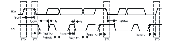 Figure 6. I2C Interface Timing
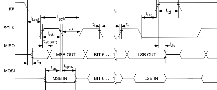
8.18 SPI Interface Timing (See Figure 7)
| IOVDD = 1.8V | IOVDD = 3.3V | UNIT | |||||||
|---|---|---|---|---|---|---|---|---|---|
| MIN | TYP | MAX | MIN | TYP | MAX | ||||
| tsck | SCLK Period(1) | 100 | 50 | ns | |||||
| tsckh | SCLK Pulse width High | 50 | 25 | ns | |||||
| tsckl | SCLK Pulse width Low | 50 | 25 | ns | |||||
| tlead | Enable Lead Time | 30 | 20 | ns | |||||
| ttrail | Enable Trail Time | 30 | 20 | ns | |||||
| td;seqxfr | Sequential Transfer Delay | 40 | 20 | ns | |||||
| ta | Slave DOUT access time | 40 | 20 | ns | |||||
| tdis | Slave DOUT disable time | 40 | 20 | ns | |||||
| tsu | DIN data setup time | 15 | 10 | ns | |||||
| th(DIN) | DIN data hold time | 15 | 10 | ns | |||||
| tv(DOUT) | DOUT data valid time | 25 | 18 | ns | |||||
| tr | SCLK Rise Time | 4 | 4 | ns | |||||
| tf | SCLK Fall Time | 4 | 4 | ns | |||||
8.19 Typical Characteristics
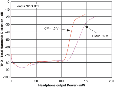 Figure 10. Total Harmonic Distortion vs Headphone Output Power
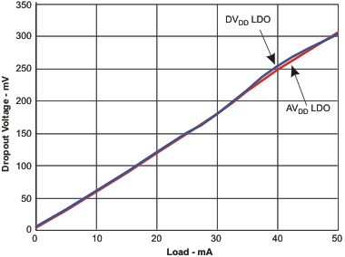 Figure 12. LDO Dropout Voltage vs Load Current
| CM = 0.9 V |
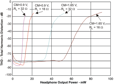 Figure 9. Total Harmonic Distortion vs Headphone Output Power
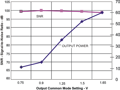 Figure 11. Headphone SNR and Output Power vs Output Common Mode Setting
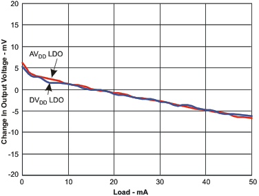 Figure 13. LDO Load Response
8.20 Typical Characteristics, FFT
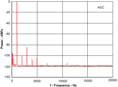 Figure 15. Single Ended Line Input to ADC FFT at -1dBr vs Frequency
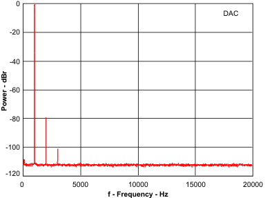 Figure 17. DAC Playback to Line-out FFT at -1dBFS vs Frequency
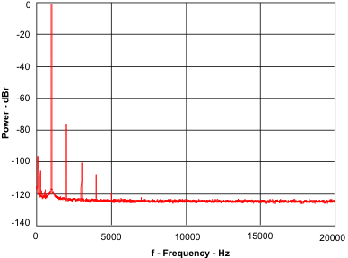 Figure 19. Line Input to Line-out FFT at 446mVrms vs Frequency
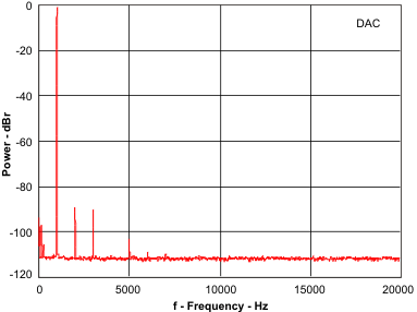 Figure 16. DAC Playback to Headphone FFT at -1dBFS vs Frequency
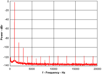 Figure 18. Line Input to Headphone FFT at 446mVrms vs Frequency