ZHCSNE0B March 2021 – February 2024 TLIN2029A-Q1
PRODUCTION DATA
- 1
- 1 特性
- 2 應(yīng)用
- 3 說明
- 4 Pin Configuration and Functions
- 5 Specifications
- 6 Parameter Measurement Information
-
7 Detailed Description
- 7.1 Overview
- 7.2 Functional Block Diagram
- 7.3
Feature Description
- 7.3.1 LIN (Local Interconnect Network) Bus
- 7.3.2 TXD (Transmit Input and Output)
- 7.3.3 RXD (Receive Output)
- 7.3.4 VSUP (Supply Voltage)
- 7.3.5 GND (Ground)
- 7.3.6 EN (Enable Input)
- 7.3.7 Protection Features
- 7.3.8 TXD Dominant Time Out (DTO)
- 7.3.9 Bus Stuck Dominant System Fault: False Wake Up Lockout
- 7.3.10 Thermal Shutdown
- 7.3.11 Under Voltage on VSUP
- 7.3.12 Unpowered Device and LIN Bus
- 7.4 Device Functional Modes
- 8 Application Information Disclaimer
- 9 Device and Documentation Support
- 10Revision History
- 11Mechanical, Packaging, and Orderable Information
封裝選項(xiàng)
機(jī)械數(shù)據(jù) (封裝 | 引腳)
散熱焊盤機(jī)械數(shù)據(jù) (封裝 | 引腳)
- DRB|8
訂購信息
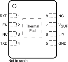
4 Pin Configuration and Functions
Figure 4-1 D
Package, 8-Pin (SOIC)
(Top View)
(Top View)
 Figure 4-2 DRB
Package, 8-Pin (VSON)
Figure 4-2 DRB
Package, 8-Pin (VSON)(Top View)
Table 4-1 Pin Functions
| PIN | TYPE | DESCRIPTION | |
|---|---|---|---|
| NAME | NO. | ||
| RXD | 1 | DO | RXD output (open-drain) interface reporting state of LIN bus voltage |
| EN | 2 | DI | Enable input - High puts the device in normal operation mode and low puts the device in sleep mode |
| NC | 3 | – | Not connected |
| TXD | 4 | DI | TXD input interface to control state of LIN output - Internally pulled to ground |
| GND | 5 | GND | Ground |
| LIN | 6 | HV I/O | LIN bus single-wire transmitter and receiver |
| VSUP | 7 | HV Supply | Device supply voltage (connected to battery in series with external reverse blocking diode) |
| NC | 8 | – | Not connected |
| Thermal Pad | - | Can be connected to the PCB ground plane to improve thermal coupling (DRB package only) | |