ZHCSRU3J January 2008 – March 2023 SN65HVD1785 , SN65HVD1786 , SN65HVD1787 , SN65HVD1791 , SN65HVD1792 , SN65HVD1793
PRODUCTION DATA
- 1 特性
- 2 應(yīng)用
- 3 說(shuō)明
- 4 Revision History
- 5 Product Selection Guide
- 6 Pin Configuration and Functions
- 7 Specifications
- 8 Parameter Measurement Information
- 9 Detailed Description
- 10Application and Implementation
- 11Power Supply Recommendations
- 12Layout
- 13Device and Documentation Support
- 14Mechanical, Packaging, and Orderable Information
封裝選項(xiàng)
機(jī)械數(shù)據(jù) (封裝 | 引腳)
- D|14
散熱焊盤機(jī)械數(shù)據(jù) (封裝 | 引腳)
訂購(gòu)信息
6 Pin Configuration and Functions
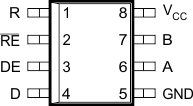
 Figure 6-1 D or P Package
8-Pin SOIC or PDIP
SN65HVD1785, 1786, 1787 (Top View)
Pin Functions
(SN65HVD1785, SN65HVD1786, SN65HVD1787)
| PIN | TYPE | DESCRIPTION | |
|---|---|---|---|
| NAME | NO. | ||
| A | 6 | Bus input/output | Driver output or receiver input (complementary to B) |
| B | 7 | Bus input/output | Driver output or receiver input (complementary to A) |
| D | 4 | Digital input | Driver data input |
| DE | 3 | Digital input | Driver enable, active high |
| GND | 5 | Reference potential | Local device ground |
| R | 1 | Digital output | Receive data output |
| RE | 2 | Digital input | Receiver enable, active low |
| VCC | 8 | Supply | 4.5-V-to-5.5-V supply |

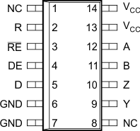
NC - No internal
connection
Pins 6 and 7 are connected together internally.
Pins 13 and 14 are connected together internally.
Figure 6-2 D PackagePins 6 and 7 are connected together internally.
Pins 13 and 14 are connected together internally.
14-Pin SOIC
SN65VD1791, 1792, 1793 (Top View)
Pin Functions
(SN65HVD1791, SN65HVD1792, SN65HVD1793)
| PIN | TYPE | DESCRIPTION | |
|---|---|---|---|
| NAME | NO. | ||
| A | 12 | Bus input | Receiver input (complementary to B) |
| B | 11 | Bus input | Receiver input (complementary to A) |
| Y | 9 | Bus output | Driver output (complementary to Z) |
| Z | 10 | Bus output | Driver output (complementary to Y) |
| D | 5 | Digital input | Driver data input |
| DE | 4 | Digital input | Driver enable, active high |
| GND | 6, 7 | Reference potential | Local device ground |
| R | 2 | Digital output | Receive data output |
| RE | 3 | Digital input | Receiver enable, active low |
| VCC | 13, 14 | Supply | 4.5-V to 5.5-V supply |
| NC | 1, 8 | No connect | No connect; should be left floating |