SLLS877H December 2007 – March 2017 SN65HVD1780 , SN65HVD1781 , SN65HVD1782
PRODUCTION DATA.
- 1 Features
- 2 Applications
- 3 Description
- 4 Revision History
- 5 Device Comparison Table
- 6 Pin Configuration and Functions
- 7 Specifications
- 8 Parameter Measurement Information
- 9 Detailed Description
- 10Application and Implementation
- 11Power Supply Recommendations
- 12Layout
- 13Device and Documentation Support
- 14Mechanical, Packaging, and Orderable Information
封裝選項(xiàng)
機(jī)械數(shù)據(jù) (封裝 | 引腳)
散熱焊盤機(jī)械數(shù)據(jù) (封裝 | 引腳)
訂購信息
8 Parameter Measurement Information
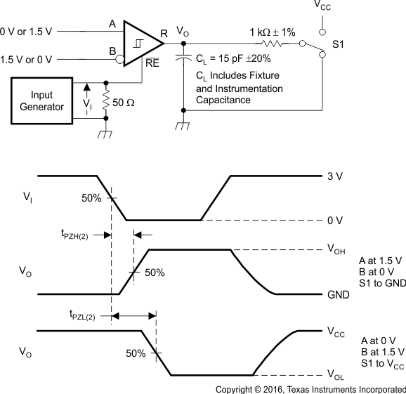
Input generator rate is 100 kbps, 50% duty cycle, rise or fall time is less than 6 ns, output impedance is 50 Ω.
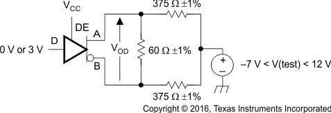 Figure 6. Measurement of Driver Differential Output Voltage With Common-Mode Load
 Figure 7. Measurement of Driver Differential and Common-Mode Output With RS-485 Load
 Figure 8. Measurement of Driver Differential Output Rise and Fall Times and Propagation Delays

NOTE:
D at 3 V to test non-inverting output, D at 0 V to test inverting output.
NOTE:
D at 0 V to test non-inverting output, D at 3 V to test inverting output.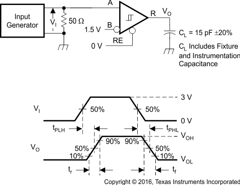 Figure 11. Measurement of Receiver Output Rise and Fall Times and Propagation Delays
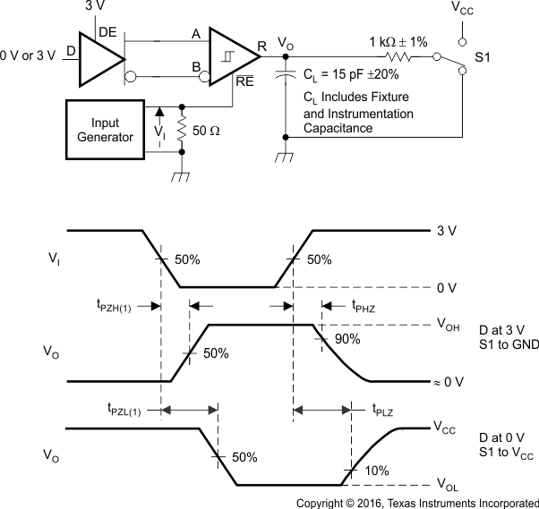 Figure 12. Measurement of Receiver Enable and Disable Times With Driver Enabled
8.1 Equivalent Input Schematic
When the input digital pins float, internal high value resistors pull D/REB pins to VCC and DE pin to GND to place the device into known states. If the voltage level of D/REB input pins is higher than that of power rail, input current can flow through the input resistor and pull up resistor to VCC.
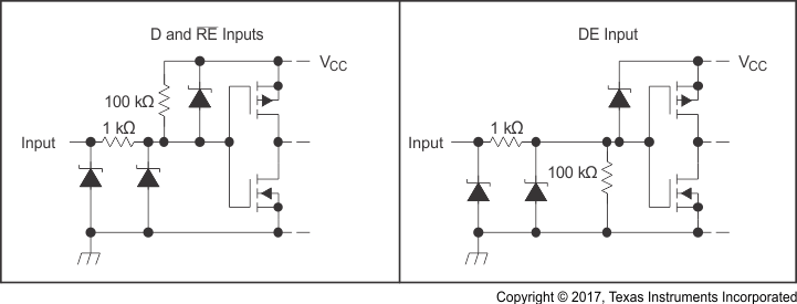 Figure 14. Equivalent Input Schematic Diagrams
