ZHCS234B August 2012 – January 2016 PCM5141 , PCM5142
PRODUCTION DATA.
- 1 特性
- 2 應(yīng)用
- 3 說明
- 4 修訂歷史記錄
- 5 Device Comparison
- 6 Pin Configuration and Functions
-
7 Specifications
- 7.1 Absolute Maximum Ratings
- 7.2 ESD Ratings
- 7.3 Recommended Operating Conditions
- 7.4 Thermal Information
- 7.5 Electrical Characteristics
- 7.6 Timing Requirements: SCK Input
- 7.7 Timing Requirements: PCM Audio Data
- 7.8 Timing Requirements: I2S Master
- 7.9 Timing Requirements: XSMT
- 7.10 Switching Characteristics
- 7.11 Typical Characteristics
-
8 Detailed Description
- 8.1 Overview
- 8.2 Functional Block Diagram
- 8.3
Feature Description
- 8.3.1 Terminology
- 8.3.2 Audio Data Interface
- 8.3.3 XSMT Pin (Soft Mute / Soft Un-Mute)
- 8.3.4 Audio Processing
- 8.3.5 DAC Outputs
- 8.3.6
Reset and System Clock Functions
- 8.3.6.1 Clocking Overview
- 8.3.6.2 Clock Slave Mode With Master and System Clock (SCK) Input (4 Wire I2S)
- 8.3.6.3 Clock Slave Mode With BCK PLL to Generate Internal Clocks (3-Wire PCM)
- 8.3.6.4 Clock Generation Using the PLL
- 8.3.6.5 PLL Calculation
- 8.3.6.6 Clock Master Mode from Audio Rate Master Clock
- 8.3.6.7 Clock Master from a Non-Audio Rate Master Clock
- 8.4 Device Functional Modes
- 8.5 Programming
- 9 Application and Implementation
- 10Power Supply Recommendations
- 11Layout
- 12Register Maps
- 13器件和文檔支持
- 14機械、封裝和可訂購信息
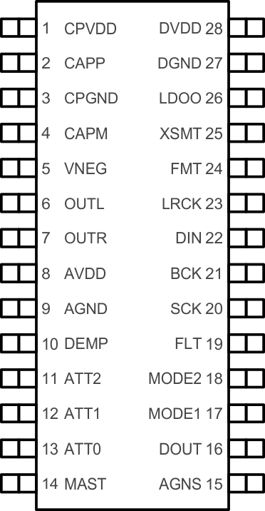
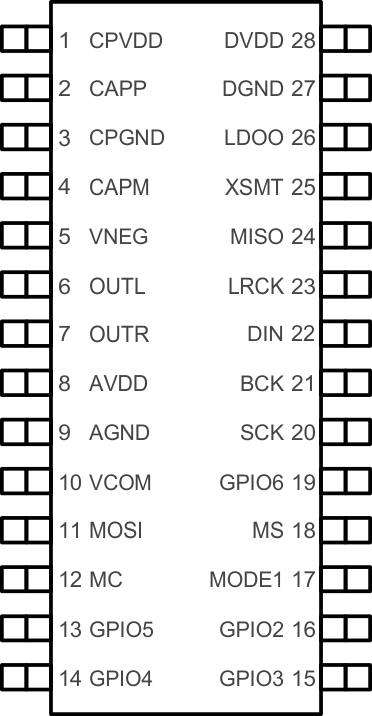
6 Pin Configuration and Functions
RHB Package
I2C Mode
(MODE1 tied to DGND and MODE2 tied to DVDD)
Top View

RHB Package
Hardwired Mode
(MODE1 tied to DGND, MODE2 tied to DGND)
Top View

RHB Package
SPI Mode
(MODE1 tied to DVDD)
Top View

Table 3. Gain and Attenuation in Hardwired Mode
| ATT PIN CONDITION (ATT2 : ATT1 : ATT0) | GAIN AND ATTENUATION LEVEL |
|---|---|
| ( 0 0 0 ) | 0 dB |
| ( 0 0 1 ) | 3 dB |
| ( 0 1 0 ) | 6 dB |
| ( 0 1 1 ) | 9 dB |
| ( 1 0 0 ) | 12 dB |
| ( 1 0 1 ) | 15 dB |
| ( 1 1 0 ) | –6 dB |
| ( 1 1 1 ) | –3 dB |
6.1 Pin Functions
| PIN | I/O | DESCRIPTION | |||||
|---|---|---|---|---|---|---|---|
| NAME | MODE, NO. | ||||||
| I2C | SPI | HW | |||||
| CPVDD | 1 | 1 | 1 | - | Charge pump power supply, 3.3 V | ||
| CAPP | 2 | 2 | 2 | O | Charge pump flying capacitor terminal for positive rail | ||
| CPGND | 3 | 3 | 3 | - | Charge pump ground | ||
| CAPM | 4 | 4 | 4 | O | Charge pump flying capacitor terminal for negative rail | ||
| VNEG | 5 | 5 | 5 | O | Negative charge pump rail terminal for decoupling, –3.3 V | ||
| OUTL | 6 | 6 | 6 | O | Analog output from DAC left channel | ||
| OUTR | 7 | 7 | 7 | O | Analog output from DAC right channel | ||
| AVDD | 8 | 8 | 8 | - | Analog power supply, 3.3 V | ||
| AGND | 9 | 9 | 9 | - | Analog ground | ||
| VCOM | 10 | 10 | – | O | I2C, SPI | VCOM output (optional mode selected by register; default setting is VREF mode.) When in VREF mode (default), this pin ties to GND. When in VCOM mode, decoupling capacitor to GND is required. | |
| DEMP | – | – | 10 | I | HW | DEMP: De-emphasis control for 44.1-kHz sampling rate: Off (Low) / On (High) | |
| SDA | 11 | – | – | I/O | I2C | Data for I2C(1)(2) | |
| MOSI | – | 11 | – | I | SPI | Input data for SPI(2) | |
| ATT2 | – | – | 11 | HW | Digital gain and attenuation control pin | ||
| SCL | 12 | – | – | I | I2C | Input clock for I2C(2) | |
| MC | – | 12 | – | SPI | Input clock for SPI(2) | ||
| ATT1 | – | – | 12 | HW | Digital gain and attenuation control pin | ||
| GPIO5 | 13 | 13 | – | I/O | I2C, SPI | General purpose digital input and output port (3) | |
| ATT0 | – | – | 13 | HW | Digital gain and attenuation control pin | ||
| GPIO4 | 14 | 14 | – | I/O | I2C, SPI | General purpose digital input and output port (3) | |
| MAST | – | – | 14 | HW | I2S Master clock select pin : Master (High) BCK/LRCK outputs, Slave (Low) BCK/LRCK inputs | ||
| GPIO3 | 15 | 15 | – | I/O | I2C, SPI | General purpose digital input and output port (3) | |
| AGNS | – | – | 15 | HW | Analog gain selector : 0-dB 2-VRMS output (Low), –6-dB 1-VRMS output (High) | ||
| ADR2 | 16 | – | – | I/O | I2C | 2nd LSB address select bit for I2C | |
| GPIO2 | – | 16 | – | SPI | General purpose digital input and output port | ||
| DOUT | – | – | 16 | O | HW | General Purpose Output (Low level) | |
| MODE1 | 17 | 17 | 17 | I | Mode control selection pin (2)
MODE1 = Low, MODE2 = Low : Hardwired mode MODE1 = Low, MODE2 = High: I2C mode MODE1 = High: SPI mode |
||
| MODE2 | 18 | – | 18 | I2C, HW | MODE2 | ||
| MS | – | 18 | – | I | SPI | MS pin (chip select for SPI) | |
| GPIO6 | 19 | 19 | – | I/O | I2C, SPI | General purpose digital input and output port | |
| FLT | – | – | 19 | I | HW | Filter select : Normal latency (Low) / Low latency (High) | |
| SCK | 20 | 20 | 20 | I | System clock input(2) | ||
| BCK | 21 | 21 | 21 | I/O | Audio data bit clock input (slave) or output (master)(2) | ||
| DIN | 22 | 22 | 22 | I | Audio data input(2) | ||
| LRCK | 23 | 23 | 23 | I/O | Audio data word clock input (slave) or output (master)(2) | ||
| ADR1 | 24 | – | – | I/O | I2C | LSB address select bit for I2C | |
| MISO (GPIO1) | – | 24 | – | SPI | Primary output data for SPI readback. Secondary; general purpose digital input/output port controlled by register | ||
| FMT | – | – | 24 | HW | Audio format selection : I2S (Low) / Left justified (High) | ||
| XSMT | 25 | 25 | 25 | I | Soft mute control Soft mute(2) (Low) / soft un-mute (High) | ||
| LDOO | 26 | 26 | 26 | - | Internal logic supply rail terminal for decoupling, 1.8 V | ||
| DGND | 27 | 27 | 27 | - | Digital ground | ||
| DVDD | 28 | 28 | 28 | - | Digital power supply, 3.3 V or 1.8 V | ||
(1) Open-drain configuration in out mode.
(2) Failsafe LVCMOS Schmitt trigger input.
(3) Internal Pulldown