SBAS448B October 2008 – August 2015 PCM1690
PRODUCTION DATA.
- 1 Features
- 2 Applications
- 3 Description
- 4 Revision History
- 5 Pin Configuration and Functions
-
6 Specifications
- 6.1 Absolute Maximum Ratings
- 6.2 ESD Ratings
- 6.3 Recommended Operating Conditions
- 6.4 Thermal Information
- 6.5 Electrical Characteristics: Digital Input/Output
- 6.6 Electrical Characteristics: DAC
- 6.7 Electrical Characteristics: Power-Supply Requirements
- 6.8 System Clock Timing Requirements
- 6.9 Audio Interface Timing Requirements for Left-Justified, Right-Justified, and I2S Data Formats
- 6.10 Audio Interface Timing Requirements for DSP and TDM Data Formats
- 6.11 Three-Wire Serial Control Interface Timing Requirements
- 6.12 SCL and SDA Control Interface Timing Requirements
- 6.13 Typical Characteristics
-
7 Detailed Description
- 7.1 Overview
- 7.2 Functional Block Diagram
- 7.3
Feature Description
- 7.3.1 Analog Outputs
- 7.3.2 Voltage Reference VCOM
- 7.3.3 System Clock Input
- 7.3.4 Sampling Mode
- 7.3.5 Reset Operation
- 7.3.6 Zero Flag
- 7.3.7 AMUTE Control
- 7.3.8 Three-Wire (SPI) Serial Control
- 7.3.9 Control Data Word Format
- 7.3.10 Register Write Operation
- 7.3.11 Two-Wire (I2C) Serial Control
- 7.3.12 Packet Protocol
- 7.3.13 Write Operation
- 7.3.14 Read Operation
- 7.3.15 Timing Requirements: SCL and SDA
- 7.4 Device Functional Modes
- 7.5 Register Maps
- 8 Application and Implementation
- 9 Power Supply Recommendations
- 10Layout
- 11Device and Documentation Support
- 12Mechanical, Packaging, and Orderable Information
封裝選項
請參考 PDF 數據表獲取器件具體的封裝圖。
機械數據 (封裝 | 引腳)
- DCA|48
散熱焊盤機械數據 (封裝 | 引腳)
- DCA|48
訂購信息
6 Specifications
6.1 Absolute Maximum Ratings
Over operating free-air temperature range (unless otherwise noted).(1)| PARAMETER | MIN | MAX | UNIT | |
|---|---|---|---|---|
| Supply voltage | VCC1, VCC2 | –0.3 | 6.5 | V |
| VDD | –0.3 | 4 | V | |
| Ground voltage differences | AGND1, AGND2, DGND | –0.1 | 0.1 | V |
| Supply voltage differences | VCC1, VCC2 | –0.1 | 0.1 | V |
| Digital input voltage | RST, TEST, MS, MC, MD, SCKI, AMUTEI, AMUTEO | –0.3 | 6.5 | V |
| BCK, LRCK, DIN1/2/3/4, MODE, ZERO1, ZERO2 | –0.3 | (VDD + 0.3) < 4 | V | |
| Analog input voltage | VCOM, VOUT1–8± | –0.3 | (VCC + 0.3) < 6.5 | V |
| Input current | (all pins except supplies) | –10 | 10 | mA |
| Ambient temperature under bias | –40 | 125 | °C | |
| Junction temperature | 150 | °C | ||
| Lead temperature | (soldering, 5s) | 260 | °C | |
| Package temperature | (IR reflow, peak) | 260 | °C | |
| Storage temperature | Tstg | –55 | 150 | °C |
(1) Stresses beyond those listed under Absolute Maximum Ratings may cause permanent damage to the device. These are stress ratings only and functional operation of the device at these or any other conditions beyond those indicated under Recommended Operating Conditions is not implied. Exposure to absolute-maximum-rated conditions for extended periods may affect device reliability.
6.2 ESD Ratings
| VALUE | UNIT | |||
|---|---|---|---|---|
| V(ESD) | Electrostatic discharge | Human body model (HBM), per ANSI/ESDA/JEDEC JS-001(1) | ±1000 | V |
| Charged-device model (CDM), per JEDEC specification JESD22-C101(2) | ±250 | |||
(1) JEDEC document JEP155 states that 500-V HBM allows safe manufacturing with a standard ESD control process.
(2) JEDEC document JEP157 states that 250-V CDM allows safe manufacturing with a standard ESD control process.
6.3 Recommended Operating Conditions
Over operating free-air temperature range (unless otherwise noted).| MIN | NOM | MAX | UNIT | ||
|---|---|---|---|---|---|
| Analog supply voltage, VCC | 4.5 | 5 | 5.5 | V | |
| Digital supply voltage, VDD | 3 | 3.3 | 3.6 | V | |
| Digital Interface | LVTTL compatible | ||||
| Digital input clock frequency | Sampling frequency, LRCK | 8 | 192 | kHz | |
| System clock frequency, SCKI | 2.048 | 36.864 | MHz | ||
| Analog output voltage | Differential | 8 | VPP | ||
| Analog output load resistance | To AC-coupled GND | 5 | kΩ | ||
| To DC-coupled GND | 15 | kΩ | |||
| Analog output load capacitance | 50 | pF | |||
| Digital output load capacitance | 20 | pF | |||
| Operating free-air temperature | PCM1690 consumer grade | –40 | 25 | 85 | °C |
6.4 Thermal Information
| THERMAL METRIC(1) | PCM1690 | UNIT | |
|---|---|---|---|
| DCA (HTSSOP) | |||
| 48 PINS | |||
| RθJA | Junction-to-ambient thermal resistance | 29.2 | °C/W |
| RθJC(top) | Junction-to-case (top) thermal resistance | 10.2 | °C/W |
| RθJB | Junction-to-board thermal resistance | 10.3 | °C/W |
| ψJT | Junction-to-top characterization parameter | 0.3 | °C/W |
| ψJB | Junction-to-board characterization parameter | 10.2 | °C/W |
| RθJC(bot) | Junction-to-case (bottom) thermal resistance | 0.4 | °C/W |
(1) For more information about traditional and new thermal metrics, see the Semiconductor and IC Package Thermal Metrics application report, SPRA953.
6.5 Electrical Characteristics: Digital Input/Output
All specifications at TA = 25°C, VCC1 = VCC2 = 5 V, VDD = 3.3 V, fS = 48 kHz, SCKI = 512 fS, 24-bit data, and Sampling Mode = Auto, unless otherwise noted.| PARAMETER | TEST CONDITIONS | MIN | TYP | MAX | UNIT | ||
|---|---|---|---|---|---|---|---|
| DATA FORMAT | |||||||
| fS | Sampling frequency | 8 | 48 | 192 | kHz | ||
| System clock frequency | 128 fS, 192 fS, 256 fS, 384 fS, 512 fS, 768 fS, 1152 fS |
2.048 | 36.864 | MHz | |||
| INPUT LOGIC | |||||||
| VIH | Input logic level, high (BCK, LRCK, and DIN (2)(1)) | 2 | VDD | VDC | |||
| VIL | Input logic level, low (BCK, LRCK, and DIN ((2)(1)) | 0.8 | VDC | ||||
| VIH | Input logic current, high (SCKI, ADR5/ADR1/RSV, MC/SCL/FMT, MD/SDA/DEMP, and AMUTEI(3)(4)) | 2 | 5.5 | VDC | |||
| VIL | Input logic current, low (SCKI, ADR5/ADR1/RSV, MC/SCL/FMT, MD/SDA/DEMP, and AMUTEI(3)(4)) | 0.8 | VDC | ||||
| IIH | Input logic current, high (SCKI, TEST/ADR1/RSV, MC/SCL/FMT, MD/SDA/DEMP, and AMUTEI(1)(3)) | VIN = VDD | ±10 | μA | |||
| IIL | Input logic current, low (SCKI, TEST/ADR1/RSV, MC/SCL/FMT, MD/SDA/DEMP, and AMUTEI(1)(3)) | VIN = 0 V | ±10 | μA | |||
| IIH | Input logic current, high (BCK, LRCK, REST, MSI/ADR0/RSV (2)(4)) | VIN = VDD | 65 | 100 | μA | ||
| IIL | Input logic current, high (BCK, LRCK, REST, MSI/ADR0/RSV (2)(4)) | VIN = 0 V | ±10 | μA | |||
| OUTPUT LOGIC | |||||||
| VOH | Output logic level, high (ZERO1 and ZERO2(5)) | IOUT = –4 mA | 2.4 | VDC | |||
| VOL | Output logic level, low (ZERO1 and ZERO2(5)(6) ) | IOUT = +4 mA | 0.4 | VDC | |||
| REFERENCE OUTPUT | |||||||
| VCOM output voltage | 0.5 × VCC1 | V | |||||
| VCOM output impedance | 7.5 | kΩ | |||||
| Allowable VCOM output source/sink current | 1 | μA | |||||
(1) DIN1/2/3/4 (Schmitt trigger input).
(2) BCK and LRCK (Schmitt trigger input with 50-kΩ typical internal pull-down resistor).
(3) SCKI, TEST/ADR1/RSV, MC/SCL/FMT, MD/SDA/DEMP, and AMUTEI (Schmitt trigger input, 5-V tolerant).
(4) RST and MS/ADR0/RSV (Schmitt trigger input with 50-kΩ typical internal pull-down resistor, 5-V tolerant).
(5) ZERO1 and ZERO2.
(6) SDA (I2C mode, open-drain low output) and AMUTEO (open-drain low output).
6.6 Electrical Characteristics: DAC
All specifications at TA = 25°C, VCC1 = VCC2 = 5 V, VDD = 3.3 V, fS = 48 kHz, SCKI = 512 fS, 24-bit data, and Sampling Mode = Auto, unless otherwise noted.| PARAMETER | TEST CONDITIONS | MIN | TYP | MAX | UNIT | ||
|---|---|---|---|---|---|---|---|
| RESOLUTION | 16 | 24 | Bits | ||||
| DC ACCURACY | |||||||
| Gain mismatch channel-to-channel | ±2 | ±6 | % of FSR | ||||
| Gain error | ±2 | ±6 | % of FSR | ||||
| Bipolar zero error | ±1 | % of FSR | |||||
| DYNAMIC PERFORMANCE(1)(2) | |||||||
| THD+N | Total harmonic distortion + noise | fS = 48 kHz, VOUT = 0 dB | –94 | –88 | dB | ||
| fS = 96 kHz, VOUT = 0 dB | –94 | dB | |||||
| fS = 192 kHz, VOUT = 0 dB | –94 | dB | |||||
| Dynamic range | fS = 48 kHz, EIAJ, A-weighted | 106 | 113 | dB | |||
| fS = 96 kHz, EIAJ, A-weighted | 113 | dB | |||||
| fS = 192 kHz, EIAJ, A-weighted | 113 | dB | |||||
| SNR | Sighnal-to-noise ratio | fS = 48 kHz, EIAJ, A-weighted | 106 | 113 | dB | ||
| fS = 96 kHz, EIAJ, A-weighted | 113 | dB | |||||
| fS = 192 kHz, EIAJ, A-weighted | 113 | dB | |||||
| Channel separation (between one channel and others) |
fS = 48 kHz | 103 | 109 | dB | |||
| fS = 96 kHz | 109 | dB | |||||
| fS = 192 kHz | 108 | dB | |||||
| ANALOG OUTPUT | |||||||
| Output voltage | Differential | 1.6 × VCC1 | VPP | ||||
| Center voltage | 0.5 × VCC1 | V | |||||
| Load impedance | To AC-coupled GND(3) | 5 | kΩ | ||||
| To DC-coupled GND(3) | 15 | kΩ | |||||
| LPF frequency response | f = 20 kHz | –0.04 | dB | ||||
| f = 44 kHz | –0.18 | dB | |||||
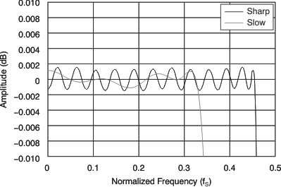
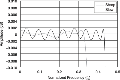
| DIGITAL FILTER PERFORMANCE WITH SHARP ROLL-OFF | |||||||
| Passband (single, dual) | Except SCKI = 128 fS and 192 fS | 0.454 × fS | Hz | ||||
| SCKI = 128 fS and 192 fS | 0.432 × fS | Hz | |||||
| Passband (quad) | 0.432 × fS | Hz | |||||
| Stop band (single, dual) | Except SCKI = 128 fS and 192 fS | 0.546 × fS | Hz | ||||
| SCKI = 128 fS and 192 fS | 0.569 × fS | Hz | |||||
| Stop band (quad) | 0.569 × fS | Hz | |||||
| Passband ripple | < 0.454 × fS, 0.432 × fS | ±0.0018 | dB | ||||
| Stop band attenuation | > 0.546 × fS, 0.569 × fS | –75 | dB | ||||
| DIGITAL FILTER PERFORMANCE WITH SLOW ROLL-OFF | |||||||
| Passband | 0.328 × fS | Hz | |||||
| Stop band | 0.673 × fS | Hz | |||||
| Passband ripple | < 0.328 × fS | ±0.0013 | dB | ||||
| Stop band attenuation | > 0.673 × fS | –75 | dB | ||||
| DIGITAL FILTER PERFORMANCE | |||||||
| Group delay time (single, dual) | Except SCKI = 128 fS and 192 fS | 28/fS | s | ||||
| SCKI = 128 fS and 192 fS | 19/fS | s | |||||
| Group delay time (quad) | 19/fS | s | |||||
| De-emphasis error | ±0.1 | dB | |||||
(1) In differential mode at VOUTx± pin, fOUT = 1 kHz, using Audio Precision System II, Average mode with 20-kHz LPF and 400-Hz HPF.
(2) fS = 48 kHz: SCKI = 512 fS (single), fS = 96 kHz : SCKI = 256 fS (dual), fS = 192 kHz : SCKI = 128 fS (quad).
(3) Allowable minimum input resistance of differential to single-ended converter with D to S Gain = G is calculated as (1 + 2G)/(1 + G) × 5k for AC-coupled and (1+ 0.9G)/(1 + G) × 15k for DC-coupled connection; refer to Figure 39 and Figure 40 of the Application Information section.
6.7 Electrical Characteristics: Power-Supply Requirements
All specifications at TA = 25°C, VCC1 = VCC2 = 5 V, VDD = 3.3 V, fS = 48 kHz, SCKI = 512 fS, 24-bit data, and Sampling Mode = Auto, unless otherwise noted.| PARAMETER | TEST CONDITIONS | MIN | TYP | MAX | UNIT | |||
|---|---|---|---|---|---|---|---|---|
| POWER-SUPPLY REQUIREMENTS | ||||||||
| VCC1/2 | Voltage range | 4.5 | 5 | 5.5 | VDC | |||
| VDD | 3 | 3.3 | 3.6 | VDC | ||||
| ICC | Supply current | fS = 48 kHz | 74 | 110 | mA | |||
| fS = 192 kHz | 74 | mA | ||||||
| Full power-down(1) | 170 | μA | ||||||
| fS = 48 kHz | 57 | 90 | mA | |||||
| IDD | fS = 192 kHz | 76 | mA | |||||
| Full power-down(1) | 60 | μA | ||||||
| Power dissipation | fS = 48 kHz fS = 192 kHz Full power-down(1) | 558 | 847 | mW | ||||
| 621 | mW | |||||||
| 1.05 | mW | |||||||
| TEMPERATURE RANGE | ||||||||
| Operating temperature | PCM1690 Consumer grade | –40 | 85 | °C | ||||
(1) SCKI, BCK, and LRCK stopped.
6.8 System Clock Timing Requirements
(see Figure 1)| MIN | MAX | UNIT | ||
|---|---|---|---|---|
| tSCY | System clock cycle time | 27 | ns | |
| tSCH | System clock width high | 10 | ns | |
| tSCL | System clock width low | 10 | ns | |
| — | System clock duty cycle | 40% | 60% | |
6.9 Audio Interface Timing Requirements for Left-Justified, Right-Justified, and I2S Data Formats
(see Figure 2)| MIN | MAX | UNIT | ||
|---|---|---|---|---|
| tBCY | BCK cycle time | 75 | ns | |
| tBCH | BCK pulse width high | 35 | ns | |
| tBCL | BCK pulse width low | 35 | ns | |
| tLRS | LRCK set-up time to BCK rising edge | 10 | ns | |
| tLRH | LRCK hold time to BCK rising edge | 10 | ns | |
| tDIS | DIN1/2/3/4 set-up time to BCK rising edge | 10 | ns | |
| tDIH | DIN1/2/3/4 hold time to BCK rising edge | 10 | ns | |
6.10 Audio Interface Timing Requirements for DSP and TDM Data Formats
(see Figure 3)| MIN | MAX | UNIT | ||
|---|---|---|---|---|
| tBCY | BCK cycle time | 40 | ns | |
| tBCH | BCK pulse width high | 15 | ns | |
| tBCL | BCK pulse width low | 15 | ns | |
| tLRW | LRCK pulse width high (DSP format) | tBCY | tBCY | |
| LRCK pulse width high (TDM format) | tBCY | 1/fS – tBCY | ||
| tLRS | LRCK set-up time to BCK rising edge | 10 | ns | |
| tLRH | LRCK hold time to BCK rising edge | 10 | ns | |
| tDIS | DIN1/2/3/4 set-up time to BCK rising edge | 10 | ns | |
| tDIH | DIN1/2/3/4 hold time to BCK rising edge | 10 | ns | |
6.11 Three-Wire Serial Control Interface Timing Requirements
(see Figure 4)| MIN | MAX | UNIT | ||
|---|---|---|---|---|
| tMCY | MC pulse cycle time | 100 | ns | |
| tMCL | MC low-level time | 40 | ns | |
| tMCH | MC high-level time | 40 | ns | |
| tMHH | MS high-level time | tMCY | ns | |
| tMSS | MS falling edge to MC rising edge | 30 | ns | |
| tMSH | MS rising edge from MC rising edge for LSB | 15 | ns | |
| tMDH | MD hold time | 15 | ns | |
| tMDS | MD set-up time | 15 | ns | |
6.12 SCL and SDA Control Interface Timing Requirements
(see Figure 5)| STANDARD MODE | FAST MODE | UNIT | ||||
|---|---|---|---|---|---|---|
| MIN | MAX | MIN | MAX | |||
| fSCL | SCL clock frequency | 100 | 400 | kHz | ||
| tBUF | Bus free time between STOP and START condition | 4.7 | 1.3 | μs | ||
| tLOW | Low period of the SCL clock | 4.7 | 1.3 | μs | ||
| tHI | High period of the SCL clock | 4 | 0.6 | μs | ||
| tS-SU | Set-up time for START/Repeated START condition | 4.7 | 0.6 | μs | ||
| tS-HD | Hold time for START/Repeated START condition | 4.0 | 0.6 | μs | ||
| tD-SU | Data set-up time | 250 | 100 | ns | ||
| tD-HD | Data hold time | 0 | 3450 | 0 | 900 | ns |
| tSCL-R | Rise time of SCL signal | 1000 | 20 + 0.1 CB | 300 | ns | |
| tSCL-F | Fall time of SCL signal | 1000 | 20 + 0.1 CB | 300 | ns | |
| tSDA-R | Rise time of SDA signal | 1000 | 20 + 0.1 CB | 300 | ns | |
| tSDA-F | Fall time of SDA signal | 1000 | 20 + 0.1 CB | 300 | ns | |
| tP-SU | Set-up time for STOP condition | 4 | 0.6 | μs | ||
| tGW | Allowable glitch width | N/A | 50 | |||
| CB | Capacitive load for SDA and SCL line | 400 | 100 | pF | ||
| VNH | Noise margin at high level for each connected device (including hysteresis) |
0.2 × VDD | 0.2 × VDD | V | ||
| VNL | Noise margin at low level for each connected device (including hysteresis) |
0.1 × VDD | 0.1 × VDD | V | ||
| VHYS | Hysteresis of Schmitt trigger input | N/A | 0.05 × VDD | V | ||
 Figure 1. System Clock Timing Requirements
 Figure 2. Audio Interface Timing Requirements for Left-Justified, Right-Justified, and I2S Data Formats
 Figure 3. Audio Interface Timing Requirements for DSP and TDM Data Formats
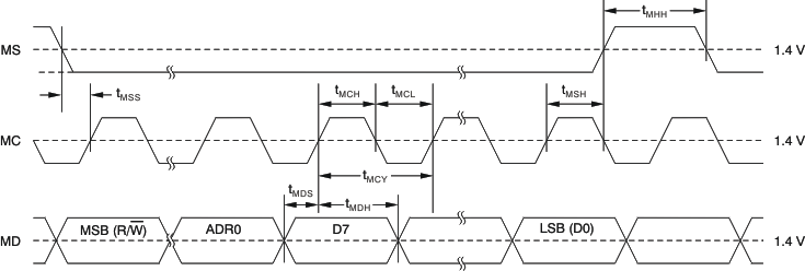 Figure 4. Three-Wire Serial Control Interface Timing
 Figure 5. SCL and SDA Control Interface Timing
6.13 Typical Characteristics
6.13.1 Digital Filter
All specifications at TA = 25°C, VCC1 = VCC2 = 5 V, VDD = 3.3 V, fS = 48 kHz, SCKI = 512 fS, 24-bit data, and Sampling Mode = Auto, unless otherwise noted.

(Single Rate)
(Dual Rate)
(Quad Rate)
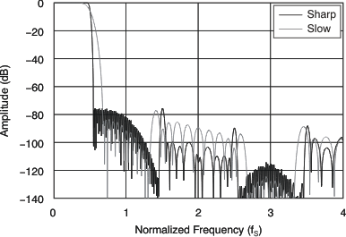
(Dual Rate)

(Quad Rate)
6.13.2 Digital De-Emphasis Filter
All specifications at TA = 25°C, VCC1 = VCC2 = 5 V, VDD = 3.3 V, fS = 48 kHz, SCKI = 512 fS, 24-bit data, and Sampling Mode = Auto, unless otherwise noted.

| fS = 48 kHz |

| fS = 32 kHz |

| fS = 44.1 kHz |

6.13.3 Dynamic Performance
All specifications at TA = 25°C, VCC1 = VCC2 = 5 V, VDD = 3.3 V, fS = 48 kHz, SCKI = 512 fS, 24-bit data, and Sampling Mode = Auto, unless otherwise noted.
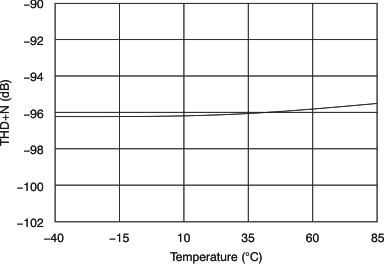
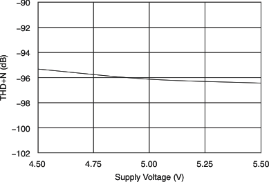
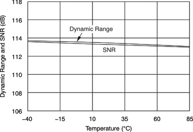
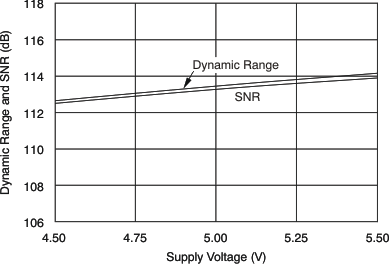
6.13.4 Output Spectrum
All specifications at TA = 25°C, VCC1 = VCC2 = 5 V, VDD = 3.3 V, fS = 48 kHz, SCKI = 512 fS, 24-bit data, and Sampling Mode = Auto, unless otherwise noted.
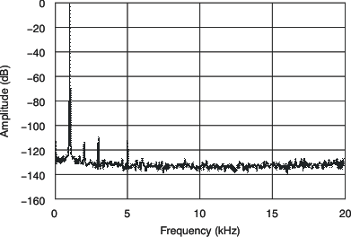
| 0 dB, N = 32768 |
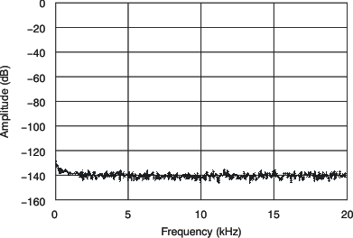
| BPZ, N = 32768 |
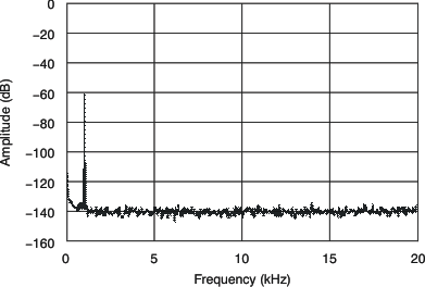
| –60 dB, N = 32768 |