ZHCSFO1H September 2008 – April 2016 LMP8601 , LMP8601-Q1 , LMP8602 , LMP8602-Q1 , LMP8603 , LMP8603-Q1
PRODUCTION DATA.
- 1 特性
- 2 應(yīng)用
- 3 說明
- 4 修訂歷史記錄
- 5 Pin Configuration and Functions
- 6 Specifications
- 7 Detailed Description
- 8 Application and Implementation
- 9 Power Supply Recommendations
- 10Layout
- 11器件和文檔支持
- 12機(jī)械、封裝和可訂購信息
封裝選項(xiàng)
機(jī)械數(shù)據(jù) (封裝 | 引腳)
- D|8
散熱焊盤機(jī)械數(shù)據(jù) (封裝 | 引腳)
訂購信息
6 Specifications
6.1 Absolute Maximum Ratings
over operating free-air temperature range (unless otherwise noted)(1)| MIN | MAX | UNIT | ||
|---|---|---|---|---|
| Supply voltage (VS – GND) | –0.3 | 6 | V | |
| Continuous input voltage (–IN and +IN) | –22 | 60 | V | |
| Transient (400 ms) | –25 | 65 | V | |
| Maximum voltage at A1, A2, OFFSET and OUT pins | VS + 0.3 | GND – 0.3 | V | |
| Operating temperature, TA | LMP8601EDRQ1 only | –40 | 150 | °C |
| All other devices | –40 | 125 | ||
| Junction temperature(2) | –40 | 150 | °C | |
| Mounting temperature | Infrared or convection (20 sec) | 235 | °C | |
| Wave soldering lead (10 sec) | 260 | |||
| Storage temperature, Tstg | –65 | 150 | °C | |
(1) Stresses beyond those listed under Absolute Maximum Ratings may cause permanent damage to the device. These are stress ratings only, which do not imply functional operation of the device at these or any other conditions beyond those indicated under Recommended Operating Conditions. Exposure to absolute-maximum-rated conditions for extended periods may affect device reliability.
(2) The maximum power dissipation must be derated at elevated temperatures and is dictated by TJ(MAX), RθJA, and the ambient temperature, TA. The maximum allowable power dissipation PDMAX = (TJ(MAX) – TA) / RθJA or the number given in Absolute Maximum Ratings, whichever is lower.
6.2 ESD Ratings: LMP860x
| VALUE | UNIT | ||||
|---|---|---|---|---|---|
| V(ESD) | Electrostatic discharge | Human body model (HBM), per ANSI/ESDA/JEDEC JS-001(1) | All pins except 1 and 8 | ±2000 | V |
| Pins 1 and 8 | ±4000 | ||||
| Charged-device model (CDM), per JEDEC specification JESD22-C101(2) | ±1000 | ||||
| Machine model | ±200 | ||||
(1) JEDEC document JEP155 states that 500-V HBM allows safe manufacturing with a standard ESD control process.
(2) JEDEC document JEP157 states that 250-V CDM allows safe manufacturing with a standard ESD control process.
6.3 ESD Ratings: LMP860x-Q1
| VALUE | UNIT | ||||
|---|---|---|---|---|---|
| V(ESD) | Electrostatic discharge | Human body model (HBM), per AEC Q100-002(1) | All pins except 1 and 8 | ±2000 | V |
| Pins 1 and 8 | ±4000 | ||||
| Charged-device model (CDM), per AEC Q100-011 | ±1000 | ||||
| Machine model | ±200 | ||||
(1) AEC Q100-002 indicates that HBM stressing shall be in accordance with the ANSI/ESDA/JEDEC JS-001 specification.
6.4 Recommended Operating Conditions
over operating free-air temperature range (unless otherwise noted)| MIN | MAX | UNIT | ||
|---|---|---|---|---|
| Supply voltage (VS – GND) | 3 | 5.5 | V | |
| OFFSET voltage (Pin 7) | 0 | VS | V | |
| Operating temperature, TA (1) | LMP8601EDRQ1 only | –40 | 150 | °C |
| All other devices | –40 | 125 | ||
(1) The maximum power dissipation must be derated at elevated temperatures and is dictated by TJ(MAX), RθJA, and the ambient temperature, TA. The maximum allowable power dissipation PDMAX = (TJ(MAX) – TA) / RθJA or the number given in Absolute Maximum Ratings, whichever is lower.
6.5 Thermal Information
| THERMAL METRIC(1) | LMP860x, LMP860x-Q1 | LMP8602, LMP8602-Q1, LMP8603, LMP8603-Q1 | UNIT | |
|---|---|---|---|---|
| D (SOIC) | DGK (VSSOP) | |||
| 8 PINS | 8 PINS | |||
| RθJA | Junction-to-ambient thermal resistance(2) | 113.1 | 171.1 | °C/W |
| RθJC(top) | Junction-to-case (top) thermal resistance | 57.3 | 64.1 | °C/W |
| RθJB | Junction-to-board thermal resistance | 53.5 | 91.1 | °C/W |
| ψJT | Junction-to-top characterization parameter | 11.1 | 9.4 | °C/W |
| ψJB | Junction-to-board characterization parameter | 53.0 | 89.7 | °C/W |
| RθJC(bot) | Junction-to-case (bottom) thermal resistance | N/A | N/A | °C/W |
(1) For more information about traditional and new thermal metrics, see the Semiconductor and IC Package Thermal Metrics application report, SPRA953.
(2) The maximum power dissipation must be derated at elevated temperatures and is dictated by TJ(MAX), RθJA, and the ambient temperature, TA. The maximum allowable power dissipation PDMAX = (TJ(MAX) – TA) / RθJA or the number given in Absolute Maximum Ratings, whichever is lower.
6.6 Electrical Characteristics: VS = 3.3 V
at TA = 25°C, VS = 3.3 V, GND = 0 V, –4 V ≤ VCM ≤ 27 V, RL = ∞, OFFSET (pin 7) is grounded, and 10 nF between VS and GND (unless otherwise noted)| PARAMETER | TEST CONDITIONS | MIN(1) | TYP(2) | MAX(1) | UNIT | |||
|---|---|---|---|---|---|---|---|---|
| OVERALL PERFORMANCE (FROM -IN (PIN 1) AND +IN (PIN 8) TO OUT (PIN 5) WITH PINS A1 (PIN 3) AND A2 (PIN 4) CONNECTED) | ||||||||
| IS | Supply current | 1 | mA | |||||
| Over full temperature range | 0.6 | 1.3 | ||||||
| AV | Total gain | LMP8601, LMP8601-Q1 | 19.9 | 20 | 20.1 | V/V | ||
| LMP8602, LMP8602-Q1 | 49.75 | 50 | 50.25 | |||||
| LMP8603, LMP8603-Q1 | 99.5 | 100 | 100.5 | |||||
| Gain Drift(10) | Over full temperature range | –2.7 | ±20 | ppm/°C | ||||
| SR | Slew rate(3) | VIN = ±0.165 V | 0.4 | 0.7 | V/μs | |||
| BW | Bandwidth | 50 | 60 | kHz | ||||
| VOS | Input offset voltage | VCM = VS / 2 | 0.15 | ±1 | mV | |||
| TCVOS | Input offset voltage drift(4) | Over full temperature range | 2 | ±10 | μV/°C | |||
| en | Input-referred voltage noise | 0.1 Hz - 10 Hz, 6 sigma | 16.4 | μVP-P | ||||
| Spectral density, 1 kHz | 830 | nV/√Hz | ||||||
| PSRR | Power-supply rejection ratio | 3.0 V ≤ VS ≤ 3.6 V, DC, VCM = VS/2 | 86 | dB | ||||
| Over full temperature range | 70 | |||||||
| Midscale offset scaling accuracy | LMP8601, LMP8601-Q1 |
±0.15% | ±0.5% | |||||
| Input referred | ±0.413 | mV | ||||||
| LMP8602, LMP8602-Q1 |
±0.25% | ±1% | ||||||
| Input referred | ±0.33 | mV | ||||||
| LMP8603, LMP8603-Q1 |
±0.45% | ±1.5% | ||||||
| Input referred | ±0.248 | mV | ||||||
| PREAMPLIFIER (FROM INPUT PINS -IN, (PIN 1) AND +IN (PIN 8) TO A1 (PIN 3)) | ||||||||
| RCM | Input impedance common mode | –4 V ≤ VCM ≤ 27 V | 295 | kΩ | ||||
| Over full temperature range | 250 | 350 | ||||||
| RDM | Input impedance differential mode | –4 V ≤ VCM ≤ 27 V | 590 | kΩ | ||||
| Over full temperature range | 500 | 700 | ||||||
| VOS | Input offset voltage | VCM = VS / 2 | ±0.15 | ±1 | mV | |||
| DC CMRR | DC common-mode rejection ratio | –2 V ≤ VCM ≤ 24 V | 96 | dB | ||||
| Over full temperature range | 86 | |||||||
| AC CMRR | AC common-mode rejection ratio(5) | f = 1 kHz | 80 | 94 | dB | |||
| f = 10 kHz | 85 | |||||||
| CMVR | Input common-mode voltage range | for 80-dB CMRR | Over full temperature range | –4 | 27 | V | ||
| K1 | Preamplifier gain(10) | 9.95 | 10.0 | 10.05 | V/V | |||
| RF-INT | Output impedance filter resistor | 100 | kΩ | |||||
| –40°C ≤ TA ≤ 125°C | 99 | 101 | ||||||
| –40°C ≤ TA ≤ 150°C, LMP8601EDRQ1 only | 97 | 103 | ||||||
| TCRF-INT | Output impedance filter resistor drift | Over full temperature range | ±5 | ±50 | ppm/°C | |||
| A1 VOUT | A1 output voltage swing | VOL, RL = ∞ | 2 | mV | ||||
| Over full temperature range | 10 | |||||||
| VOH, RL = ∞ | 3.25 | V | ||||||
| Over full temperature range | 3.2 | |||||||
| OUTPUT BUFFER (FROM A2 (PIN 4) TO OUT (PIN 5 )) | ||||||||
| VOS | Input offset voltage | 0V ≤ VCM ≤ VS | –2 | ±0.5 | 2 | mV | ||
| Over full temperature range | –2.5 | 2.5 | ||||||
| K2 | Output buffer gain(10) | LMP8601, LMP8601-Q1 | 1.99 | 2 | 2.01 | V/V | ||
| LMP8602, LMP8602-Q1 | 4.975 | 5 | 5.025 | |||||
| LMP8603, LMP8603-Q1 | 9.95 | 10 | 10.05 | |||||
| IB | Input bias current of A2(6), | –40 | fA | |||||
| Over full temperature range | ±20 | nA | ||||||
| A2 VOUT | A2 output voltage swing(7) (8) | VOL, RL = 100 kΩ | LMP8601, LMP8601-Q1, | 4 | mV | |||
| Over full temperature range | 20 | |||||||
| LMP8602, LMP8602-Q1 | 10 | |||||||
| Over full temperature range | 40 | |||||||
| LMP8603, LMP8603-Q1 | 10 | |||||||
| Over full temperature range | 80 | |||||||
| VOH, RL = 100 kΩ | 3.29 | V | ||||||
| Over full temperature range | 3.28 | |||||||
| ISC | Output short-circuit current(9) | Sourcing, VIN = VS, VOUT = GND | –25 | –38 | –60 | mA | ||
| Sinking, VIN = GND, VOUT = VS | 30 | 46 | 65 | |||||
(2) Typical values represent the most likely parameter norms at TA = 25°C, and at the Recommended Operation Conditions at the time of product characterization.
(3) Slew rate is the average of the rising and falling slew rates.
(4) Offset voltage drift determined by dividing the change in VOS at temperature extremes into the total temperature change.
(5) AC common-mode signal is a 5-VPP sine-wave (0 V to 5 V) at the given frequency.
(6) Positive current corresponds to current flowing into the device.
(7) For this test input is driven from A1 stage.
(8) For VOL, RL is connected to VS and for VOH, RL is connected to GND.
(9) Short-Circuit test is a momentary test. Continuous short circuit operation at elevated ambient temperature can result in exceeding the maximum allowed junction temperature of 150°C.
(10) Both the gain of preamplifier K1 and the gain of buffer amplifier K2 are measured individually. The overall gain of both amplifiers (AV) is also measured to assure the gain of all parts is always within the AV limits.
6.7 Electrical Characteristics: VS = 5 V
at TA = 25°C, VS = 5 V, GND = 0 V, –22 V ≤ VCM ≤ 60 V, RL = ∞, OFFSET (pin 7) is grounded, and 10 nF between VS and GND (unless otherwise noted)| PARAMETER | TEST CONDITIONS | MIN(1) | TYP(2) | MAX(1) | UNIT | |||
|---|---|---|---|---|---|---|---|---|
| OVERALL PERFORMANCE (FROM -IN (PIN 1) AND +IN (PIN 8) TO OUT (PIN 5) WITH PINS A1 (PIN 3) AND A2 (PIN 4) CONNECTED) | ||||||||
| IS | Supply current | 1.1 | mA | |||||
| Over full temperature range | 0.7 | 1.5 | ||||||
| AV | Total gain(10) | LMP8601, LMP8601-Q1 | 19.9 | 20 | 20.1 | V/V | ||
| LMP8602, LMP8602-Q1 | 49.75 | 50 | 50.25 | |||||
| LMP8603, LMP8603-Q1 | 99.5 | 100 | 100.5 | |||||
| Gain drift | –40°C ≤ TA ≤ 125°C | –2.8 | ±20 | ppm/°C | ||||
| SR | Slew rate(3) | VIN = ±0.25 V | 0.6 | 0.83 | V/μs | |||
| BW | Bandwidth | 50 | 60 | kHz | ||||
| VOS | Input offset voltage | 0.15 | ±1 | mV | ||||
| TCVOS | Input offset voltage drift(4) | –40°C ≤ TA ≤ 125°C | 2 | ±10 | μV/°C | |||
| eN | Input-referred voltage noise | 0.1 Hz - 10 Hz, 6 sigma | 17.5 | μVP-P | ||||
| Spectral density, 1 kHz | 890 | nV/√Hz | ||||||
| PSRR | Power-supply rejection ratio | 4.5 V ≤ VS ≤ 5.5 V, DC | 90 | dB | ||||
| Over full temperature range | 70 | |||||||
| Midscale offset scaling accuracy | LMP8601, LMP8601-Q1 |
±0.15% | ±0.5% | |||||
| Input-referred | ±0.625 | mV | ||||||
| LMP8602, LMP8602-Q1 |
±0.25% | ±1% | ||||||
| Input-referred | ±0.50 | mV | ||||||
| LMP8603, LMP8603-Q1 |
±0.45% | ±1.5% | ||||||
| Input-referred | ±0.375 | mV | ||||||
| PREAMPLIFIER (FROM INPUT PINS -IN (PIN 1) AND +IN (PIN 8) TO A1 (PIN 3)) | ||||||||
| RCM | Input impedance, common mode | 0 V ≤ VCM ≤ 60 V | 295 | kΩ | ||||
| Over full temperature range | 250 | 350 | ||||||
| –20 V ≤ VCM ≤ 0 V | 193 | kΩ | ||||||
| Over full temperature range | 165 | 250 | ||||||
| RDM | Input impedance, differential mode | 0 V ≤ VCM ≤ 60 V | 590 | kΩ | ||||
| Over full temperature range | 500 | 700 | ||||||
| –20 V ≤ VCM ≤ 0 V | 386 | kΩ | ||||||
| Over full temperature range | 300 | 500 | ||||||
| VOS | Input offset voltage | VCM = VS / 2 | ±0.15 | ±1 | mV | |||
| DC CMRR | DC common-mode rejection ratio | –20 V ≤ VCM ≤ 60 V | 105 | dB | ||||
| Over full temperature range | 90 | |||||||
| AC CMRR | AC common-mode rejection ratio(5) | f = 1 kHz | 80 | 96 | dB | |||
| f = 10 kHz | 83 | |||||||
| CMVR | Input common-mode voltage range | for 80-dB CMRR | Over full temperature range | –22 | 60 | V | ||
| K1 | Preamplifier gain(10) | 9.95 | 10 | 10.05 | V/V | |||
| RF-INT | Output impedance filter resistor | 100 | kΩ | |||||
| –40°C ≤ TA ≤ 125°C, | 99 | 101 | ||||||
| –40°C ≤ TA ≤ 150°C, LMP8601EDRQ1 only | 97 | 103 | ||||||
| TCRF-INT | Output impedance filter resistor drift | ±5 | ±50 | ppm/°C | ||||
| A1 VOUT | A1 output voltage swing | VOL, RL = ∞ | 2 | mV | ||||
| Over full temperature range | 10 | |||||||
| VOH, RL = ∞ | 4.985 | V | ||||||
| Over full temperature range | 4.95 | |||||||
| OUTPUT BUFFER (FROM A2 (PIN 4) TO OUT (PIN 5)) | ||||||||
| VOS | Input offset voltage | 0V ≤ VCM ≤ VS | –2 | ±0.5 | 2 | mV | ||
| Over full temperature range | –2.5 | 2.5 | ||||||
| K2 | Output buffer gain(10) | LMP8601, LMP8601-Q1 | 1.99 | 2 | 2.01 | V/V | ||
| LMP8602, LMP8602-Q1 | 4.975 | 5 | 5.025 | |||||
| LMP8603, LMP8603-Q1 | 9.95 | 10 | 10.05 | |||||
| IB | Input bias current of A2(6) | –40 | fA | |||||
| Over full temperature range | ±20 | nA | ||||||
| A2 VOUT | A2 output voltage swing(7) (8) | VOL, RL = ∞ | LMP8601, LMP8601-Q1, | 4 | mV | |||
| Over full temperature range | 20 | |||||||
| LMP8602, LMP8602-Q1 | 10 | |||||||
| Over full temperature range | 40 | |||||||
| LMP8602, LMP8603-Q1 | 10 | |||||||
| Over full temperature range | 80 | |||||||
| VOH, RL = ∞ | 4.99 | V | ||||||
| Over full temperature range | 4.98 | |||||||
| ISC | Output short-circuit current(9) | Sourcing, VIN = VS, VOUT = GND | –25 | –42 | –60 | mA | ||
| Sinking, VIN = GND, VOUT = VS | 30 | 48 | 65 | |||||
6.8 Typical Characteristics
at TA = 25°C, VS = 5 V, GND = 0 V, –22 ≤ VCM ≤ 60 V, RL = ∞, OFFSET (pin 7) connected to VS, and 10 nF between VS and GND (unless otherwise noted)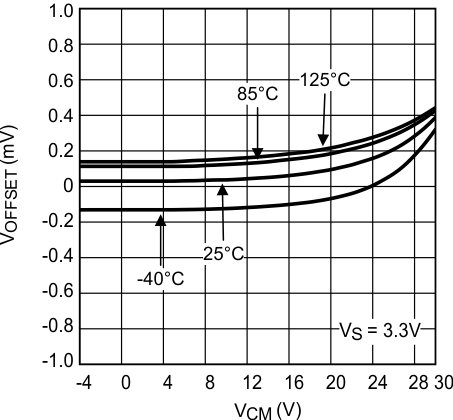
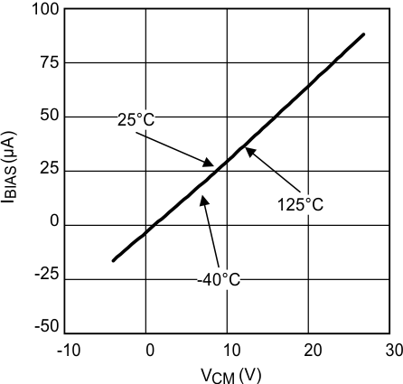 Figure 3. Input Bias Current Over Temperature (+IN and –IN pins) at VS = 3.3 V
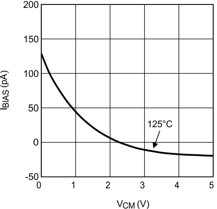 Figure 5. Input Bias Current Over Temperature (A2 pin) at VS = 5 V
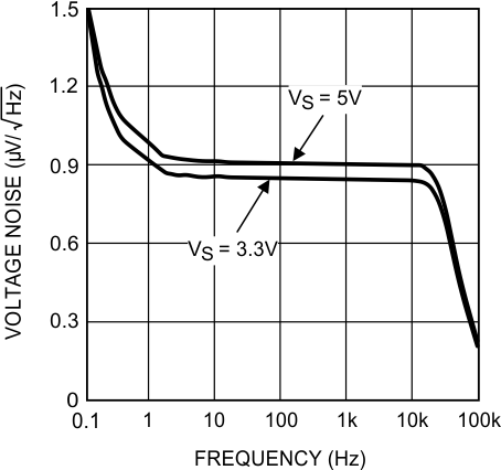 Figure 7. Input-Referred Voltage Noise vs Frequency
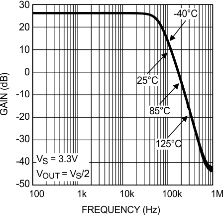 Figure 9. Gain vs Frequency at VS = 3.3 V
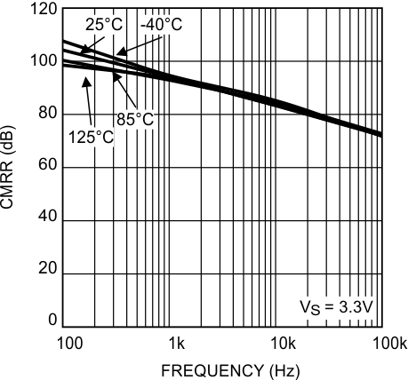 Figure 11. CMRR vs Frequency at VS = 3.3 V
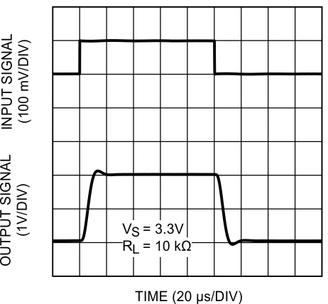 Figure 13. Step Response at VS = 3.3 V
LMP8601 and LMP8601-Q1
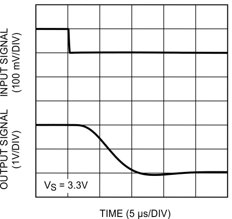 Figure 15. Settling Time (Falling Edge) at VS = 3.3 V
LMP8601 and LMP8601-Q1
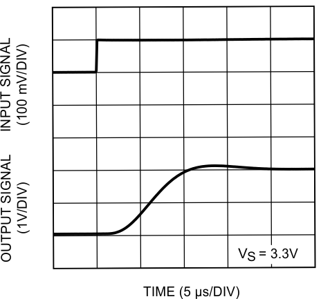 Figure 17. Settling Time (Rising Edge) at VS = 3.3 V
LMP8601 and LMP8601-Q1
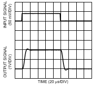 Figure 19. Step Response at VS = 3.3 V, RL = 10 kΩ
LMP8602 and LMP8602-Q1
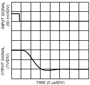 Figure 21. Settling Time (Falling Edge) at VS = 3.3 V
LMP8602 and LMP8602-Q1
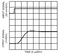 Figure 23. Settling Time (Rising Edge) at VS = 3.3 V
LMP8602 and LMP8602-Q1
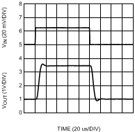 Figure 25. Step Response at VS = 3.3 V, RL = 10 kΩ
LMP8603 and LMP8603-Q1
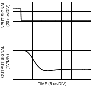 Figure 27. Settling Time (Falling Edge) at VS = 3.3 V
LMP8603 and LMP8603-Q1
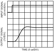 Figure 29. Settling Time (Rising Edge) at VS = 3.3 V
LMP8603 and LMP8603-Q1
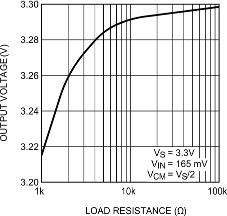 Figure 31. Positive Swing vs RLOAD at VS = 3.3 V
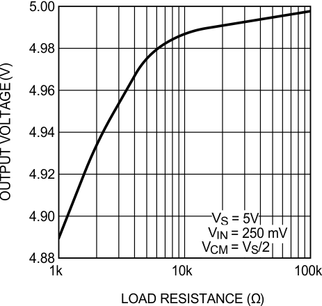 Figure 33. Positive Swing vs RLOAD VS = 5 V
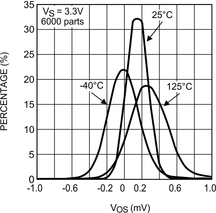 Figure 35. VOS Distribution at VS = 3.3 V
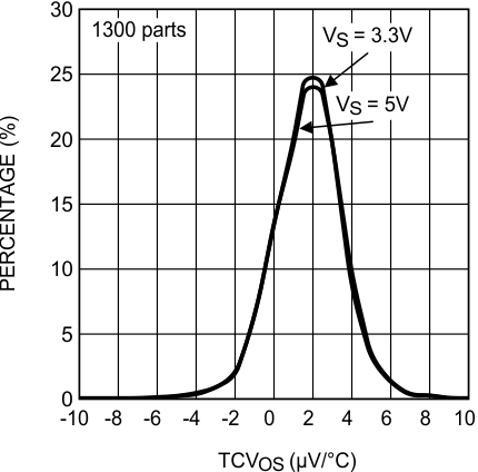 Figure 37. TCVOS Distribution
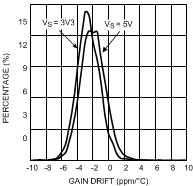 Figure 39. Gain Drift Distribution, 5000 Parts
LMP8602 and LMP8602-Q1
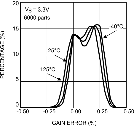 Figure 41. Gain Error Distribution at VS = 3.3 V
LMP8601 and LMP8601-Q1
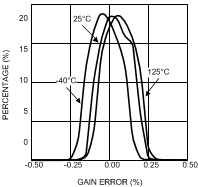 Figure 43. Gain Error Distribution at VS = 3.3 V, 5000 Parts
LMP8602 and LMP8602-Q1
 Figure 45. Gain Error Distribution at VS = 3.3 V, 5000 Parts
LMP8603 and LMP8603-Q1
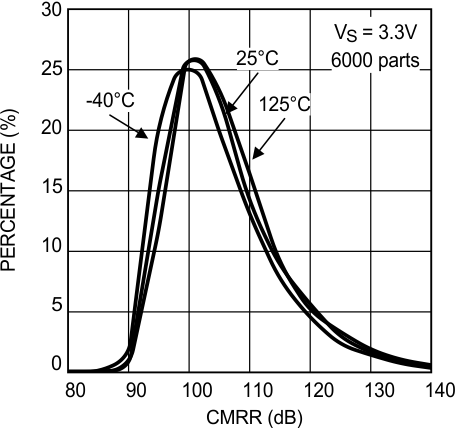 Figure 47. CMRR Distribution at VS = 3.3 V
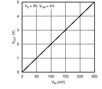
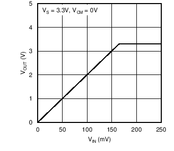 Figure 51. Output Voltage vs VIN
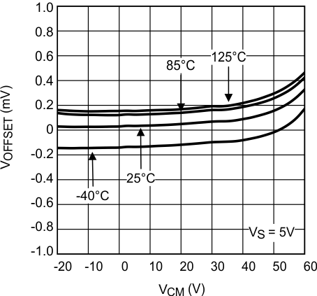
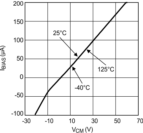 Figure 4. Input Bias Current Over Temperature (+IN and –IN pins) at VS = 5 V
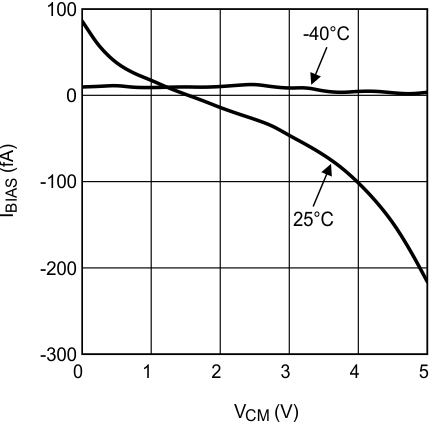 Figure 6. Input Bias Current Over Temperature (A2 pin) at VS = 5 V
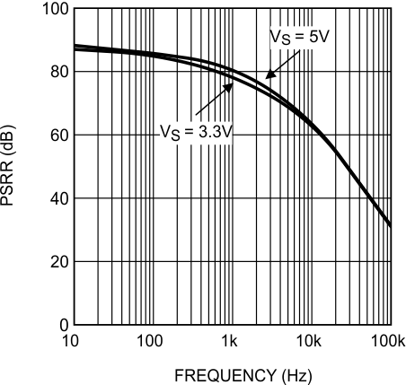 Figure 8. PSRR vs Frequency
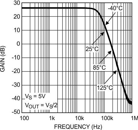 Figure 10. Gain vs Frequency at VS = 5 V
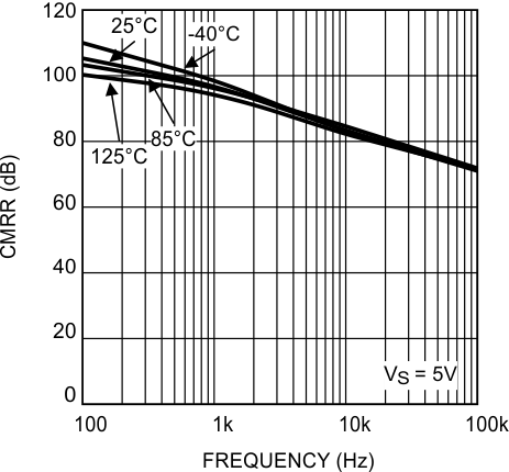 Figure 12. CMRR vs Frequency at VS = 5 V
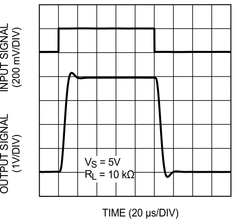 Figure 14. Step Response at VS = 5 V
LMP8601 and LMP8601-Q1
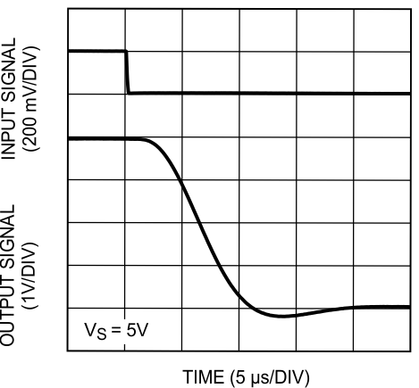 Figure 16. Settling Time (Falling Edge) at VS = 5 V
LMP8601 and LMP8601-Q1
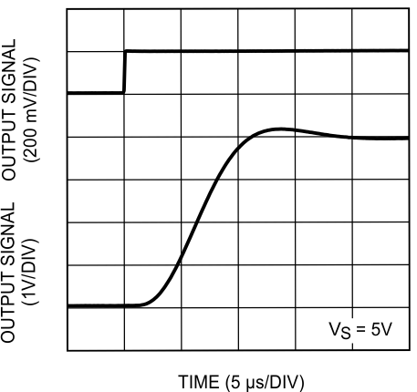 Figure 18. Settling Time (Rising Edge) at VS = 5 V
LMP8601 and LMP8601-Q1
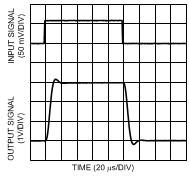 Figure 20. Step Response at VS = 5 V, RL = 10 kΩ
LMP8602 and LMP8602-Q1
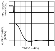 Figure 22. Settling Time (Falling Edge) at VS = 5 V
LMP8602 and LMP8602-Q1
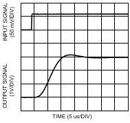 Figure 24. Settling Time (Rising Edge) at VS = 5 V
LMP8602 and LMP8602-Q1
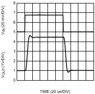 Figure 26. Step Response at VS = 5 V, RL = 10 kΩ
LMP8603 and LMP8603-Q1
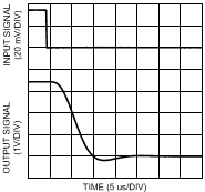 Figure 28. Settling Time (Falling Edge) at VS = 5 V
LMP8603 and LMP8603-Q1
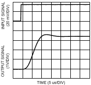 Figure 30. Settling Time (Rising Edge) at VS = 5 V
LMP8603 and LMP8603-Q1
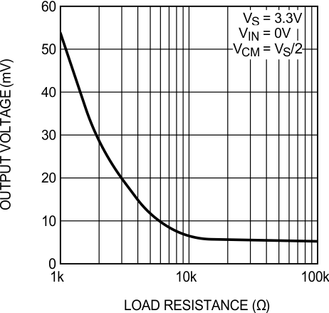 Figure 32. Negative Swing vs RLOAD at VS = 3.3 V
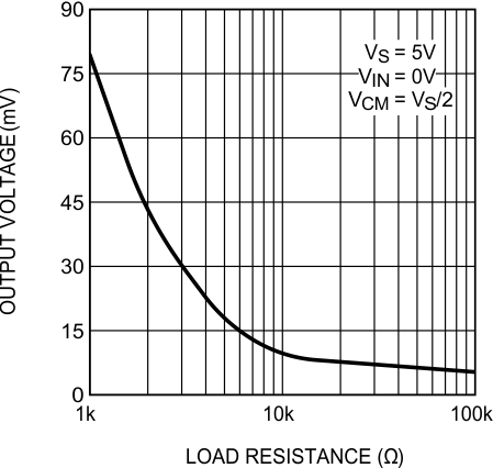 Figure 34. Negative Swing vs RLOAD at VS = 5 V
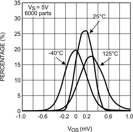 Figure 36. VOS Distribution at VS = 5 V
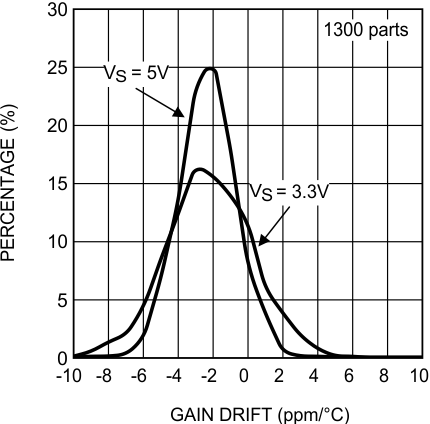 Figure 38. Gain Drift Distribution, 1300 Parts
LMP8601 and LMP8601-Q1
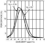 Figure 40. Gain Drift Distribution, 5000 Parts
LMP8603 and LMP8603-Q1
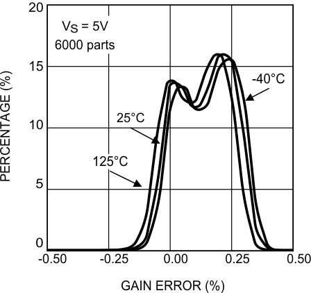 Figure 42. Gain Error Distribution at VS = 5 V
LMP8601 and LMP8601-Q1
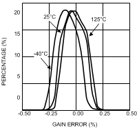 Figure 44. Gain Error Distribution at VS = 5 V, 5000 Parts
LMP8602 and LMP8602-Q1
 Figure 46. Gain Error Distribution at VS = 5 V
LMP8603 and LMP8603-Q1
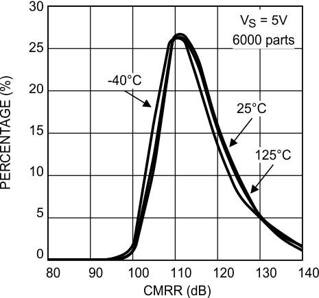 Figure 48. CMRR Distribution at VS = 5 V
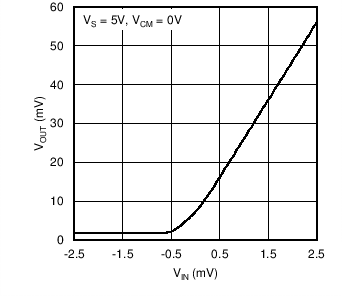 Figure 50. Output Voltage vs VIN (Enlarged Close to 0 V)
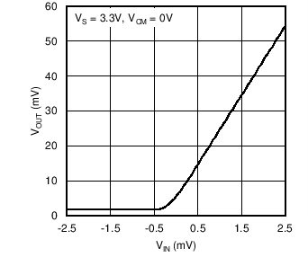 Figure 52. Output Voltage vs VIN (Enlarged Close to 0 V)
