ZHCSGG9 June 2017 LM5118-Q1
PRODUCTION DATA.
- 1 特性
- 2 應用
- 3 說明
- 4 修訂歷史記錄
- 5 Pin Configuration and Functions
- 6 Specifications
- 7 Detailed Description
-
8 Application and Implementation
- 8.1 Application Information
- 8.2
Typical Application
- 8.2.1 Design Requirements
- 8.2.2
Detailed Design Procedure
- 8.2.2.1 Custom Design With WEBENCH® Tools
- 8.2.2.2 R7 = RT
- 8.2.2.3 Inductor Selection, L1
- 8.2.2.4 R13 = RSENSE
- 8.2.2.5 C15 = CRAMP
- 8.2.2.6 Inductor Current Limit Calculation
- 8.2.2.7 C9 - C12 = Output Capacitors
- 8.2.2.8 D1
- 8.2.2.9 D4
- 8.2.2.10 C1 - C5 = Input Capacitor
- 8.2.2.11 C20
- 8.2.2.12 C8
- 8.2.2.13 C16 = CSS
- 8.2.2.14 R8, R9
- 8.2.2.15 R1, R3, C21
- 8.2.2.16 R2
- 8.2.2.17 Snubber
- 8.2.2.18 Error Amplifier Configuration
- 8.2.3 Application Curves
- 9 Power Supply Recommendations
- 10Layout
- 11器件和文檔支持
- 12機械、封裝和可訂購信息
6 Specifications
6.1 Absolute Maximum Ratings
over operating free air temperature range (unless otherwise noted)(1)| MIN | MAX | UNIT | |
|---|---|---|---|
| VIN, EN, VOUT to GND | –0.3 | 76 | V |
| VCC, LO, VCCX, UVLO to GND | –0.3 | 15 | V |
| HB to HS | –0.3 | 15 | V |
| HO to HS | –0.3 | HB + 0.3 | V |
| HS to GND | –4 | 76 | V |
| CSG, CS to GND | –0.3 | 0.3 | V |
| RAMP, SS, COMP, FB, SYNC, RT to GND | –0.3 | 7 | V |
| Junction temperature | –40 | 150 | °C |
| Storage temperature, Tstg | –55 | 150 | °C |
(1) Stresses beyond those listed under Absolute Maximum Ratings may cause permanent damage to the device. These are stress ratings only, which do not imply functional operation of the device at these or any other conditions beyond those indicated under Recommended Operating Conditions. Exposure to absolute-maximum-rated conditions for extended periods may affect device reliability.
6.2 ESD Ratings
| VALUE | UNIT | |||
|---|---|---|---|---|
| V(ESD) | Electrostatic discharge | Human-body model (HBM), per AEC Q100-002(1) | ±2000 | V |
| Charged-device model (CDM), per AEC Q100-011 | ±1000 | |||
(1) AEC Q100-002 indicates that HBM stressing shall be in accordance with the ANSI/ESDA/JEDEC JS-001 specification.
6.3 Recommended Operating Conditions
over operating free air temperature range (unless otherwise noted)(4)| MIN | MAX | UNIT | |
|---|---|---|---|
| VIN (2) | 3 | 75 | V |
| VCC, VCCX | 4.75 | 14 | V |
| Junction temperature | –40 | +125 | °C |
6.4 Thermal Information
| THERMAL METRIC(1) | LM5118-Q1 | UNIT | |
|---|---|---|---|
| PWP (HTSSOP) | |||
| 20 PINS | |||
| RθJA | Junction-to-ambient thermal resistance | 40 | °C/W |
| RθJC(bot) | Junction-to-case (bottom) thermal resistance | 4 | °C/W |
(1) For more information about traditional and new thermal metrics, see the IC Package Thermal Metrics application report.
6.5 Electrical Characteristics
Unless otherwise specified, the following conditions apply: VIN = 48 V, VCCX = 0 V, EN = 5 V, RT = 29.11 kΩ, No load on LO and HO. Typical values apply for TJ = 25°C; minimum and maximum values apply over the full junction temperature range for operation, −40°C to +125°C.(1)| PARAMETER | TEST CONDITIONS | MIN | TYP | MAX | UNIT | |
|---|---|---|---|---|---|---|
| VIN SUPPLY | ||||||
| IBIAS | VIN operating current | VCCX = 0 V | 4.5 | 5.5 | mA | |
| IBIASX | VIN operating current | VCCX = 5 V | 1 | 1.85 | mA | |
| ISTDBY | VIN shutdown current | EN = 0 V | 1 | 10 | µA | |
| VCC REGULATOR | ||||||
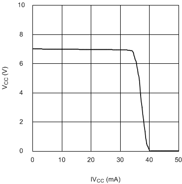
| VCC(REG) | VCC regulation | VCCX = 0 V | 6.8 | 7 | 7.2 | V |
| VCC(REG) | VCC regulation | VCCX = 0 V, VIN = 6 V | 5 | 5.25 | 5.5 | V |
| VCC sourcing current limit | VCC = 0 | 21 | 35 | mA | ||
| VCCX switch threshold | VCCX rising | 3.68 | 3.85 | 4.02 | V | |
| VCCX switch hysteresis | 0.2 | V | ||||
| VCCX switch RDS(ON) | ICCX = 10 mA | 5 | 12 | Ω | ||
| VCCX switch leakage | VCCX = 0 V | 0.5 | 1 | µA | ||
| VCCCX pulldown resistance | VCCX = 3 V | 70 | kΩ | |||
| VCC undervoltage lockout voltage | VCC rising | 3.52 | 3.7 | 3.86 | V | |
| VCC undervoltage hysteresis | 0.21 | V | ||||
| HB DC bias current | HB-HS = 15 V | 205 | 260 | µA | ||
| VC LDO mode turnoff | 10 | V | ||||
| EN INPUT | ||||||
| VIL max | EN input low threshold | 0.5 | V | |||
| VIH min | EN input high threshold | 3 | V | |||
| EN input bias current | VEN = 3 V | –1 | 1 | µA | ||
| EN input bias current | VEN = 0.5 V | –1 | 1 | µA | ||
| EN input bias current | VEN = 75 V | 50 | µA | |||
| UVLO THRESHOLDS | ||||||
| UVLO standby threshold | UVLO rising | 1.191 | 1.231 | 1.271 | V | |
| UVLO threshold hysteresis | 0.105 | V | ||||
| UVLO pullup current source | UVLO = 0 V | 5 | µA | |||
| UVLO pulldown RDS(ON) | 100 | 200 | Ω | |||
| SOFT START | ||||||
| SS current source | SS = 0V | 7.5 | 10.5 | 13.5 | µA | |
| SS to FB offset | FB = 1.23 V | 150 | mV | |||
| SS output low voltage | Sinking 100 µA, UVLO = 0 V | 7 | mV | |||
| ERROR AMPLIFIER | ||||||
| VREF | FB reference voltage | Measured at FB pin, FB = COMP |
1.212 | 1.23 | 1.248 | V |
| FB input bias current | FB = 2 V | 20 | 200 | nA | ||
| COMP sink/source current | 3 | mA | ||||
| AOL | DC gain | 80 | dB | |||
| fBW | Unity bain bandwidth | 3 | MHz | |||
| PWM COMPARATORS | ||||||
| tHO(OFF) | Forced HO off-time | 305 | 400 | 495 | ns | |
| TON(MIN) | Minimum HO on-time | 70 | ns | |||
| COMP to comparator offset | 200 | mV | ||||
| OSCILLATOR (RT PIN) | ||||||
| fSW1 | Frequency 1 | RT = 29.11 kΩ | 178 | 200 | 224 | kHz |
| fSW2 | Frequency 2 | RT = 9.525 kΩ | 450 | 515 | 575 | kHz |
| SYNC | ||||||
| Sync threshold falling | 1.3 | V | ||||
| CURRENT LIMIT | ||||||
| VCS(TH) | Cycle-by-cycle sense voltage threshold (CS-CSG) | RAMP = 0 buck mode | –103 | –125 | –147 | mV |
| VCS(THX) | Cycle-by-cycle sense voltage threshold (CS-CSG) | RAMP = 0 buck-boost mode | –218 | –255 | –300 | mV |
| CS bias current | CS = 0 V | 45 | 60 | µA | ||
| CSG bias current | CSG = 0 V | 45 | 60 | µA | ||
| Current limit fault timer | 256 | cycles | ||||
| RAMP GENERATOR | ||||||
| IR1 | RAMP current 1 | VIN = 60 V, VOUT = 10 V | 245 | 305 | 365 | µA |
| IR2 | RAMP current 2 | VIN = 12 V, VOUT = 12 V | 95 | 115 | 135 | µA |
| IR3 | RAMP current 3 | VIN = 5 V, VOUT = 12 V | 65 | 80 | 95 | µA |
| VOUT bias current | VOUT = 48 V | 245 | µA | |||
| LOW-SIDE (LO) GATE DRIVER | ||||||
| VOLL | LO low-state output voltage | ILO = 100 mA | 0.14 | 0.23 | V | |
| VOHL | LO high-state output voltage | ILO = -100 mA VOHL = VCC-VLO |
0.25 | V | ||
| LO rise time | C-load = 1 nF, VCC = 8 V | 16 | ns | |||
| LO fall time | C-load = 1 nF, VCC = 8 V | 14 | ns | |||
| IOHL | Peak LO source current | VLO = 0 V, VCC = 8 V | 2.2 | A | ||
| IOLL | Peak LO sink current | VLO = VCC = 8 V | 2.7 | A | ||
| HIGH-SIDE (HO) GATE DRIVER | ||||||
| VOLH | HO low-state output voltage | IHO = 100 mA | 0.135 | 0.21 | V | |
| VOHH | HO high-state output voltage | IHO = -100 mA, VOHH = VHB-VOH |
0.25 | V | ||
| HO rise time | C-load = 1 nF, VCC = 8 V | 14 | ns | |||
| HO fall time | C-load = 1 nF, VCC = 8 V | 12 | ns | |||
| IOHH | Peak HO source current | VHO = 0V, VCC = 8 V | 2.2 | A | ||
| IOLH | Peak HO sink current | VHO = VCC = 8 V | 3.5 | A | ||
| HB-HS undervoltage lockout | 3 | V | ||||
| BUCK-BOOST CHARACTERISTICS | ||||||
| Buck-boost mode | Buck duty cycle (3) | 69% | 75% | 80% | ||
| THERMAL | ||||||
| TSD | Thermal shutdown temperature | 165 | °C | |||
| Thermal shutdown hysteresis | 25 | °C | ||||
(1) Minimum and maximum limits are 100% production tested at 25°C. Limits over the operating temperature range are ensured through correlation using Statistical Quality Control (SQC) methods. Limits are used to calculate Average Outgoing Quality Level (AOQL).
(2) 5-V VIN is required to initially start the controller.
(3) When the duty cycle exceeds 75%, the LM5118-Q1 controller gradually phases into the Buck-Boost mode.
(4) The Recommended Operating Conditions indicate conditions for which the device is intended to be functional, but does not ensure specific performance limits. For specifications and test conditions see Electrical Characteristics.
6.6 Typical Characteristics
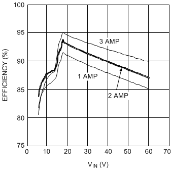
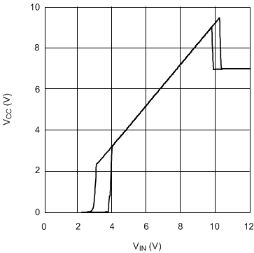
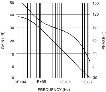
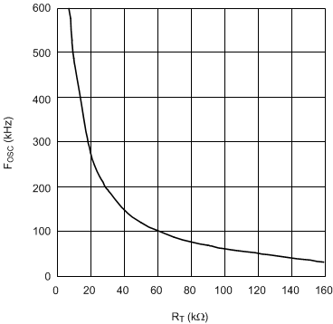
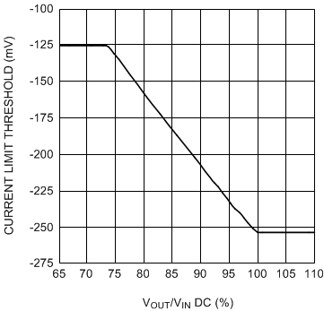
VOUT = 12 V
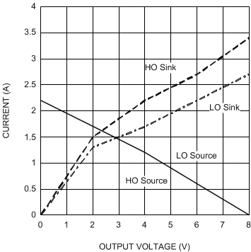
VCC = 8 V