SNVS773D April 2000 – September 2015 LM117HV , LM317HV
PRODUCTION DATA.
- 1 Features
- 2 Applications
- 3 Description
- 4 Revision History
- 5 Device Comparison Table
- 6 Pin Configuration and Functions
- 7 Specifications
- 8 Detailed Description
-
9 Application and Implementation
- 9.1 Application Information
- 9.2
Typical Applications
- 9.2.1 1.25-V to 45-V High Voltage Adjustable Regulator
- 9.2.2 Digitally Selected Outputs
- 9.2.3 Logic Regulator (5-V) With Electronic Shutdown
- 9.2.4 Slow Turnon 15-V Regulator
- 9.2.5 Adjustable Regulator With Improved Ripple Rejection
- 9.2.6 High Stability 10-V Regulator
- 9.2.7 High Current Adjustable Regulator
- 9.2.8 Emitter Follower Current Amplifier
- 9.2.9 1-A Current Regulator
- 9.2.10 Common Emitter Amplifier
- 9.2.11 Low-Cost, 3-A Switching Regulator
- 9.2.12 Adjustable Multiple On-Card Regulators With Single Control
- 9.2.13 AC Voltage Regulator
- 9.2.14 12-V Battery Charger
- 9.2.15 Adjustable 4-A Regulator
- 9.2.16 Current Limited 6-V Charger
- 10Power Supply Recommendations
- 11Layout
- 12Device and Documentation Support
- 13Mechanical, Packaging, and Orderable Information
7 Specifications
7.1 Absolute Maximum Ratings
See (1).| MIN | MAX | UNIT | ||
|---|---|---|---|---|
| Power dissipation | Internally limited | |||
| Input–output voltage differential | −0.3 | 60 | V | |
| Lead temperature (soldering, 10 seconds) | 300 | °C | ||
| Storage temperature, Tstg | −65 | 150 | °C | |
(1) Stresses beyond those listed under Absolute Maximum Ratings may cause permanent damage to the device. These are stress ratings only, which do not imply functional operation of the device at these or any other conditions beyond those indicated under Recommended Operating Conditions. Exposure to absolute-maximum-rated conditions for extended periods may affect device reliability.
7.2 ESD Ratings
| VALUE | UNIT | |||
|---|---|---|---|---|
| V(ESD) | Electrostatic discharge | Human body model (HBM)(1) | ±2000 | V |
(1) Manufacturing with less than 500-V HBM is possible with the necessary precautions.
7.3 Recommended Operating Conditions
over operating free-air temperature range (unless otherwise noted)| MIN | MAX | UNIT | |||
|---|---|---|---|---|---|
| Operating junction temperature | LM117HV | −55 | 150 | °C | |
| LM317HV | 0 | 125 | °C | ||
7.4 Thermal Information
| THERMAL METRIC(1) | LM117HV, LM317HV | LM317HV | UNIT | ||
|---|---|---|---|---|---|
| NDT (TO-39) |
NDS (TO-3) |
NDE (TO-220) |
|||
| 3 PINS | 2 PINS | 3 PINS | |||
| RθJA | Junction-to-ambient thermal resistance | 140(2) | 35(2) | 23.0 | °C/W |
| RθJC(top) | Junction-to-case (top) thermal resistance | 12 | 2.3 | 15.9 | °C/W |
| RθJB | Junction-to-board thermal resistance | — | — | 4.6 | °C/W |
| ψJT | Junction-to-top characterization parameter | — | — | 2.5 | °C/W |
| ψJB | Junction-to-board characterization parameter | — | — | 4.6 | °C/W |
| RθJC(bot) | Junction-to-case (bottom) thermal resistance | — | — | 0.9 | °C/W |
(1) For more information about traditional and new thermal metrics, see the Semiconductor and IC Package Thermal Metrics application report, SPRA953.
(2) No Heat Sink
7.5 Electrical Characteristics(1)
| PARAMETER | TEST CONDITIONS | LM117HV | LM317HV | UNIT | ||||||
|---|---|---|---|---|---|---|---|---|---|---|
| MIN | TYP | MAX | MIN | TYP | MAX | |||||
| Line Regulation | 3 V ≤ VIN − VOUT ≤ 60 V IL = 10 mA(2) |
TJ = 25°C | 0.01 | 0.02 | 0.01 | 0.04 | %/V | |||
| over full Operating Temperature Range | 0.02 | 0.05 | 0.02 | 0.07 | %/V | |||||
| Load Regulation | 10 mA ≤ IOUT ≤ IMAX | TJ = 25°C | 0.1% | 0.3% | 0.1% | 0.5% | ||||
| over full Operating Temperature Range | 0.3% | 1% | 0.3% | 1.5% | ||||||
| Thermal Regulation | TJ = 25°C, 20 ms Pulse | 0.03 | 0.07 | 0.04 | 0.07 | %/W | ||||
| Adjustment Pin Current | 50 | 100 | 50 | 100 | μA | |||||
| Adjustment Pin Current Change | 10 mA ≤ IL ≤ IMAX
3 V ≤ (VIN − VOUT) ≤ 60 V |
0.2 | 5 | 0.2 | 5 | μA | ||||
| Reference Voltage | 3 V ≤ (VIN − VOUT) ≤ 60 V 10 mA ≤ IOUT ≤ IMAX, P ≤ PMAX |
1.2 | 1.25 | 1.3 | 1.2 | 1.25 | 1.3 | V | ||
| Temperature Stability | TMIN ≤ TJ ≤ TMAX | 1% | 1% | |||||||
| Minimum Load Current | (VIN − VOUT) = 60 V | 3.5 | 7 | 3.5 | 12 | mA | ||||
| Current Limit | (VIN − VOUT) ≤ 15 V | TO-3, TO-220 Packages | 1.5 | 2.2 | 3.5 | 1.5 | 2.2 | 3.7 | A | |
| TO-39 Package | 0.5 | 0.8 | 1.8 | 0.5 | 0.8 | 1.9 | ||||
| (VIN − VOUT) ≤ 60 V | TO-3, TO-220 Packages | 0.3 | 0.3 | A | ||||||
| TO-39 Package | 0.03 | 0.03 | ||||||||
| RMS Output Noise, % of VOUT | TJ = 25°C, 10 Hz ≤ f ≤ 10 kHz | 0.003% | 0.003% | |||||||
| Ripple Rejection Ratio | VOUT = 10V, f = 120 Hz | 65 | 65 | dB | ||||||
| CADJ = 10 μF | 66 | 80 | 66 | 80 | dB | |||||
| Long-Term Stability | TJ = 125°C | 0.3% | 1% | 0.3% | 1% | |||||
(1) Unless otherwise specified, these specifications apply: −55°C ≤ TJ ≤ +150°C for the LM117HV, and 0°C ≤ TJ ≤ +125°C for the LM317HV; VIN − VOUT = 5 V and IOUT = 0.1 A for the TO-39 package and IOUT = 0.5 A for the TO-3 and TO-220 packages. Although power dissipation is internally limited, these specifications are applicable for power dissipations of 2 W for the TO-39 and 20 W for the TO-3 and TO-220. IMAX is 1.5 A for the TO-3 and TO-220 and 0.5 A for the TO-39 package.
(2) Regulation is measured at constant junction temperature. Changes in output voltage due to heating effects must be taken into account separately. Pulse testing with low duty cycle is used.
7.6 Typical Characteristics
Output capacitor = 0 μF unless otherwise noted.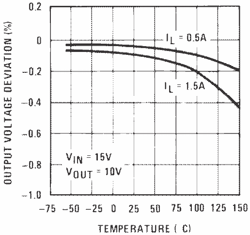 Figure 1. Load Regulation
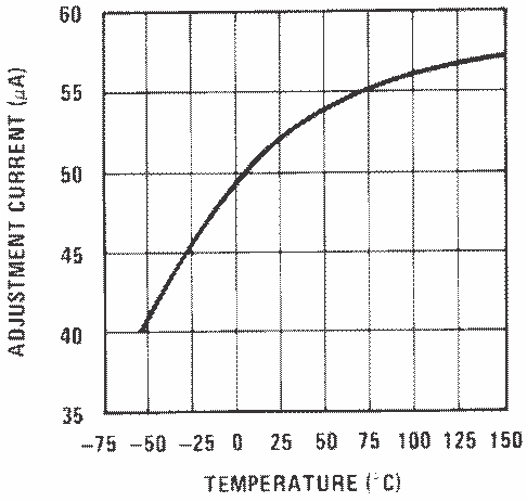 Figure 3. Adjustment Current
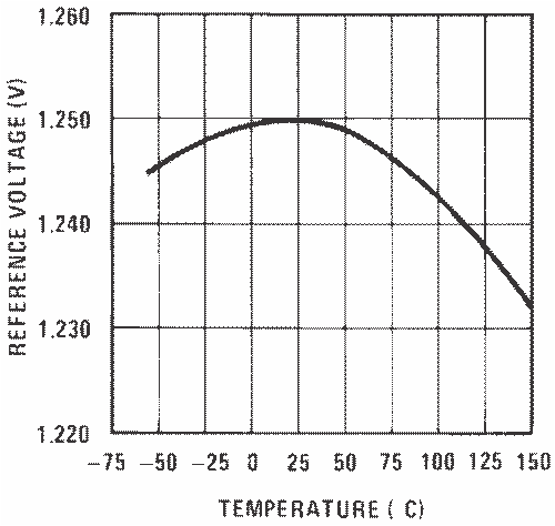 Figure 5. Temperature Stability
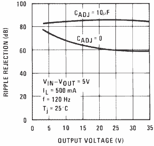 Figure 7. Ripple Rejection
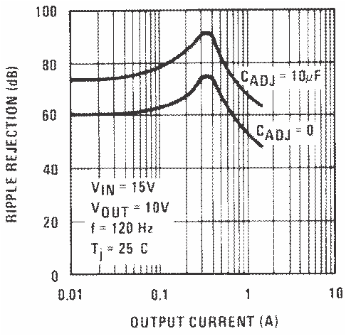 Figure 9. Ripple Rejection
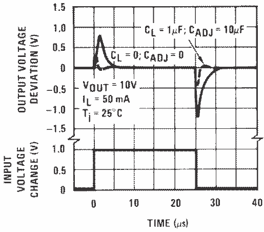 Figure 11. Line Transient Response
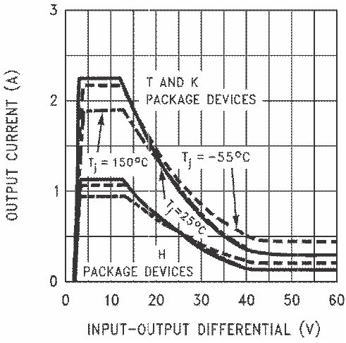 Figure 2. Current Limit
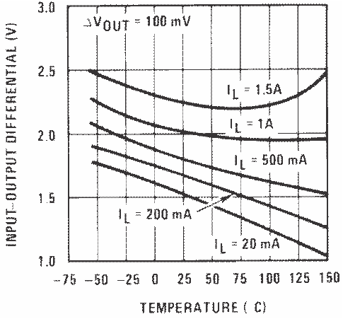 Figure 4. Dropout Voltage
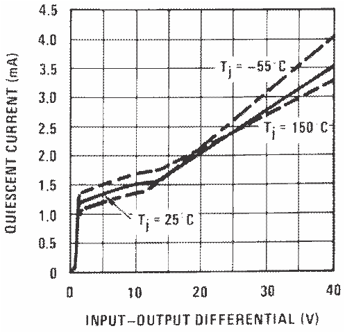 Figure 6. Minimum Operating Current
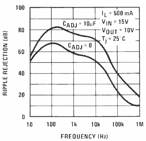 Figure 8. Ripple Rejection
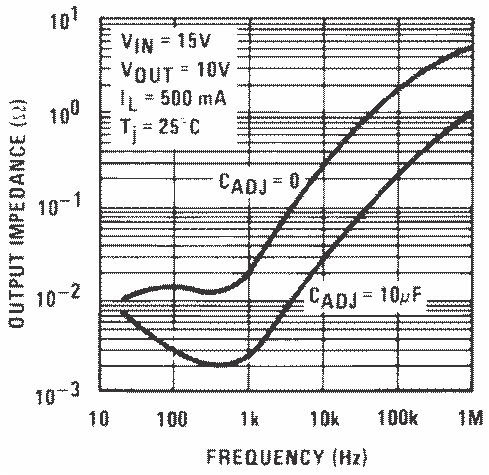 Figure 10. Output Impedance
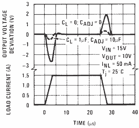 Figure 12. Load Transient Response