SNOSC66D MARCH 2012 – September 2016 LM3017
PRODUCTION DATA.
- 1 Features
- 2 Applications
- 3 Description
- 4 Revision History
- 5 Pin Configuration and Functions
- 6 Specifications
- 7 Detailed Description
-
8 Application and Implementation
- 8.1 Application Information
- 8.2
Typical Application
- 8.2.1 Design Requirements
- 8.2.2
Detailed Design Procedure
- 8.2.2.1 Programming the Output Voltage
- 8.2.2.2 Power Inductor Selection
- 8.2.2.3 Setting the Output Current
- 8.2.2.4 Additional Slope Compensation
- 8.2.2.5 Current Limit With Additional Slope Compensation
- 8.2.2.6 Power Diode Selection
- 8.2.2.7 Low-Side MOSFET Selection (Switching MOSFET)
- 8.2.2.8 Pass MOSFET Selection (High-Side MOSFET)
- 8.2.2.9 Input Capacitor Selection
- 8.2.2.10 Output Capacitor Selection
- 8.2.2.11 VCC Decoupling Capacitor
- 8.2.2.12 Slope Compensation Ramp
- 8.2.2.13 Control Loop Compensation
- 8.2.3 Application Curve
- 9 Power Supply Recommendations
- 10Layout
- 11Device and Documentation Support
- 12Mechanical, Packaging, and Orderable Information
6 Specifications
6.1 Absolute Maximum Ratings
over operating free-air temperature range (unless otherwise noted)(1)(2)| MIN | MAX | UNIT | ||
|---|---|---|---|---|
| VIN to PGND, AGND | –0.3 | 20 | V | |
| FB, COMP, VCC,DR to PGND, AGND | –0.2 | 6 | V | |
| EN/MODE | –0.2 | 5.5 | V | |
| VG | –0.3 | VIN + 6 | V | |
| ISEN to PGND, AGND | VIN – 0.3 | VIN | V | |
| Peak low side driver output current | 1 | A | ||
| Power dissipation | Internally limited | |||
| Junction temperature, TJ | 150 | °C | ||
| Storage temperature, Tstg | –65 | 150 | °C | |
(1) Stresses beyond those listed under Absolute Maximum Ratings may cause permanent damage to the device. These are stress ratings only, which do not imply functional operation of the device at these or any other conditions beyond those indicated under Recommended Operating Conditions. Exposure to absolute-maximum-rated conditions for extended periods may affect device reliability.
(2) If Military/Aerospace specified devices are required, please contact the Texas Instruments Sales Office/Distributors for availability and specifications.
6.2 ESD Ratings
| VALUE | UNIT | |||
|---|---|---|---|---|
| V(ESD) | Electrostatic discharge | Human-body model (HBM), per ANSI/ESDA/JEDEC JS-001(1) | ±1500 | V |
(1) JEDEC document JEP155 states that 500-V HBM allows safe manufacturing with a standard ESD control process.
6.3 Recommended Operating Conditions
over operating free-air temperature range (unless otherwise noted)| MIN | MAX | UNIT | ||
|---|---|---|---|---|
| VIN | Supply voltage | 5.4 | 18 | V |
| TJ | Junction temperature | –40 | 125 | °C |
6.4 Thermal Information
| THERMAL METRIC(1) | LM3017 | UNIT | |
|---|---|---|---|
| NKL (WQFN) | |||
| 10 PINS | |||
| RθJA | Junction-to-ambient thermal resistance | 79.2 | °C/W |
| RθJC(top) | Junction-to-case (top) thermal resistance | 29.8 | °C/W |
| RθJB | Junction-to-board thermal resistance | 21.4 | °C/W |
| ψJT | Junction-to-top characterization parameter | 0.6 | °C/W |
| ψJB | Junction-to-board characterization parameter | 20.7 | °C/W |
| RθJC(bot) | Junction-to-case (bottom) thermal resistance | — | °C/W |
(1) For more information about traditional and new thermal metrics, see the Semiconductor and IC Package Thermal Metrics application report.
6.5 Electrical Characteristics
Minimum and maximum limits are specified through test, design, or statistical correlation, and apply over the junction temperature range at TJ = –40°C to 125°C. Typical values are provided for reference purposes only, and represent the most likely parametric norm at TJ = 25°C. VIN = 12 V (unless otherwise noted).| PARAMETER | TEST CONDITIONS | MIN(1) | TYP(2) | MAX(1) | UNIT | |
|---|---|---|---|---|---|---|
| VFB | Feedback voltage | Vcomp = 1.4 V | 1.256 | 1.27 | 1.282 | V |
| ΔVLINE | Feedback voltage line regulation | 5 V ≤ VIN ≤ 18 V | 0.33% | |||
| VUVLO | Input undervoltage lockout voltage | Rising | 4.6 | 4.82 | 4.9 | V |
| Input undervoltage lockout hysteresis | Falling, below VUVLO | 280 | mV | |||
| FSW | Nominal switching frequency | EN/MODE = 1.6 V | 550 | 600 | 635 | kHz |
| RDS(ON) | Low-side NMOS driver resistance, top driver FET |
VIN = 5 V, IDR = 0.2 A | 3.4 | Ω | ||
| Low-side NMOS driver resistance, bottom driver FET |
VIN = 5 V, IDR = 0.2 A | 1 | ||||
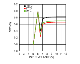
| VCC | Driver voltage supply | VIN < 6 V | VIN | V | ||
| VIN ≥ 6 V | 5.6 | |||||
| Dmax | Maximum duty cycle | 86% | ||||
| Tmin(on) | Minimum on-time | 125 | ns | |||
| IQ-boost | Supply current in boost mode, no switching |
EN/MODE = 1.6 V, FB = 1.4 V | 5.2 | 9 | mA | |
| IQ-SD | Supply current in shutdown mode | EN/MODE pin = 0.4 V | 0.025 | 1 | µA | |
| IQ-pass | Supply current in pass-through mode | EN/MODE = 2.6 V, FB = 1.4 V | 1.4 | 2.3 | mA | |
| Ven-pass | Pass-through mode threshold(3) | Rising | 2.19 | 2.4 | 2.56 | V |
| Vmode-hyst | Mode change hysteresis, falling(3) | Falling | 65 | 107 | 165 | V |
| Ven-shutdown | Shutdown mode threshold(3) | Falling | 0.2 | 0.4 | 0.59 | V |
| Ven-boost | Boost mode enable window(3) | Rising | 0.65 | 1.22 | 1.6 | V |
| Ien | EN/MODE pin bias current(4) | EN/MODE = 1.6 V | ±1 | µA | ||
| VSENSE | Cycle-by-cycle current limit threshold during boost mode | EN/MODE = 1.6 V, FB = 50 V | 142 | 170 | 182 | mV |
| ΔVSC | Short-circuit current limit threshold during boost mode | EN/MODE = 1.6 V, FB = 0 V | 18 | 30 | 42 | mV |
| VSL | Internal ramp compensation voltage | 90 | mV | |||
| VLIM1 | Input current limit threshold voltage in pass-through mode during TLIM1(3) | EN/MODE = 2.6 V | 70 | 85 | 95 | mV |
| ΔVLIM2 | Input current limit threshold voltage in pass-through mode during TLIM2(3) | EN/MODE = 2.6 V | 14.5 | 18 | 21 | mV |
| TLIM1 | Curent limit time at TLIM1(3) | 900 | µs | |||
| TLIM2 | Current limit time at TLIM2(3) | 3.6 | ms | |||
| TSC | Current limit time at TSC(3) | 900 | µs | |||
| VOVP | Upper-output overvoltage protection threshold | Rising threshold measured at FB pin with respect to FB pin, VCOMP = 1.45 V | 40 | mV | ||
| Lower-output overvoltage protection threshold | Falling threshold measured at FB pin with respect to FB pin, VCOMP = 1.45 V | 26 | ||||
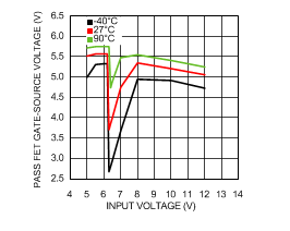
| VGS-on | On-state drive voltage at VG pin(5) | VIN = 5 V, ISEN = 5 V, IG = 0 A | 3.8 | 4.9 | V | |
| VGS-off | Off-state drive voltage at VG pin(6) | Vin = 5 V, ISEN = VIN – 200 mV, IG = 0 A | 5 | mV | ||
| IG | Maximum drive current at VG pin | VIN = 5 V, ISEN = 5 V, VG = VIN | 20 | µA | ||
| Gm | Error amplifier transconductance | VCOM = 1.4 V, ICOMP = ±50 µA | 340 | 522 | 900 | µA/V |
| AVOL | Error amplifier open-loop voltage gain | VCOM = 1.2 V to 1.8 V, ICOMP = 0 A | 190 | 313 | 450 | V/V |
| RO | Error amplifier open-loop output resistance(7) | 600 | kΩ | |||
| IEAO | Error amplifier output current swings | Sourcing: VCOMP = 1.4 V, VFB = 1.1 V | 27 | 66 | 115 | µA |
| Sinking: VCOMP = 1.4 V, VFB = 1.4 V | 49 | 68 | 125 | |||
| VEAO | Error amplifier output voltage limits | Upper: VFB = 0 V, COMP pin floating | 2.3 | V | ||
| Lower: VFB = 1.4 V | 0.82 | |||||
| Tr | Drive pin rise time | Cload = 3 nF, VDR = 0 V to 3 V | 25 | ns | ||
| Tf | Drive pin fall time | Cload = 3 nF, VDR = 3 V to 0 V | 25 | ns | ||
| TSD | Thermal shutdown threshold | 165 | °C | |||
| TSD-hyst | Thermal shutdown threshold hysteresis | 10 | °C | |||
(1) All limits are specified at room temperature and at temperature extremes. All room temperatures are 100% production tested. All limits at temperature extremes are specified through correlation using Statistical Quality Control (SQD) methods. All limits are used to calculate Average Outgoing Quaity Level (AOQL).
(2) Typical numbers are at 25°C and represent the most likely parametric norm.
(3) See Device Functional Modes and Overvoltage Protection.
(4) The bias current flowing through this pin is compensated and can flow either into or out-of this pin.
(5) This is the gate-to-source voltage drive of Q2, when the controller turns on this FET.
(6) This voltage is measured from the VG pin to AGND, when the controller fully turns off Q2.
(7) This parameter is calculated from the error amplified Gm and AVOL, and is not tested.
6.6 Typical Characteristics
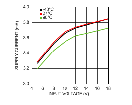
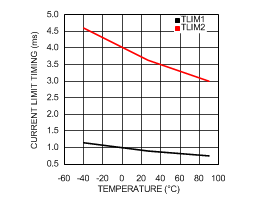
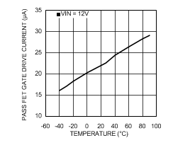
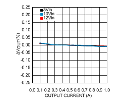
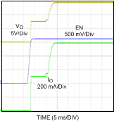
VIN = 12 V, TJ = 25°C, and see Figure 16 (unless otherwise noted).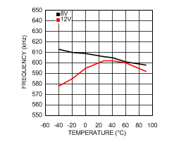
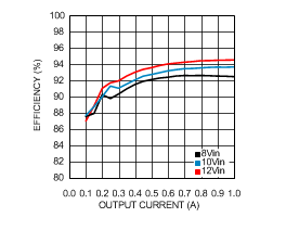
| VOUT = 15 V |
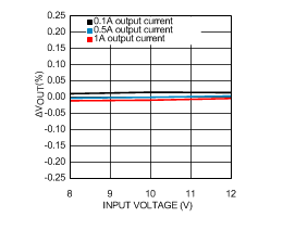
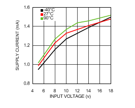
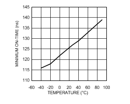
| VIN = 8 V |