ZHCSDS7A May 2015 – June 2015 LDC1101
PRODUCTION DATA.
- 1 特性
- 2 應用
- 3 說明
- 4 簡化電路原理圖
- 5 修訂歷史記錄
- 6 Pin Configuration and Functions
- 7 Specifications
-
8 Detailed Description
- 8.1 Overview
- 8.2 Functional Block Diagram
- 8.3 Feature Description
- 8.4
Device Functional Modes
- 8.4.1 Measurement Modes
- 8.4.2 RP+L Measurement Mode
- 8.4.3 High Resolution L (LHR) Measurement Mode
- 8.4.4 Reference Count Setting
- 8.4.5 L-Only Measurement Operation
- 8.4.6 Minimum Sensor Frequency and Watchdog Setting
- 8.4.7 Low Power Modes
- 8.4.8 Status Reporting
- 8.4.9 Switch Functionality and INTB Reporting
- 8.5 Programming
- 8.6
Register Maps
- 8.6.1 Individual Register Listings
- 8.6.2 Register RP_SET (address = 0x01) [reset = 0x07]
- 8.6.3 Register TC1 (address = 0x02) [reset = 0x90]
- 8.6.4 Register TC2 (address = 0x03) [reset = 0xA0]
- 8.6.5 Register DIG_CONF (address = 0x04) [reset = 0x03]
- 8.6.6 Register ALT_CONFIG (address = 0x05) [reset = 0x00]
- 8.6.7 Register RP_THRESH_HI_LSB (address = 0x06) [reset = 0x00]
- 8.6.8 Register RP_THRESH_HI_MSB (address = 0x07) [reset = 0x00]
- 8.6.9 Register RP_THRESH_LO_LSB (address = 0x08) [reset = 0x00]
- 8.6.10 Register RP_THRESH_LO_MSB (address = 0x09) [reset = 0x00]
- 8.6.11 Register INTB_MODE (address = 0x0A) [reset = 0x00]
- 8.6.12 9.Register START_CONFIG (address = 0x0B) [reset = 0x01]
- 8.6.13 Register D_CONFIG (address = 0x0C) [reset = 0x00]
- 8.6.14 Register L_THRESH_HI_LSB (address = 0x16) [reset = 0x00]
- 8.6.15 Register L_THRESH_HI_MSB (address = 0x17) [reset = 0x00]
- 8.6.16 Register L_THRESH_LO_LSB (address = 0x18) [reset = 0x00]
- 8.6.17 Register L_THRESH_LO_MSB (address = 0x19) [reset = 0x00]
- 8.6.18 Register STATUS (address = 0x020 [reset = 0x00]
- 8.6.19 Register RP_DATA_LSB (address = 0x21) [reset = 0x00]
- 8.6.20 Register RP_DATA_MSB (address = 0x22) [reset = 0x00]
- 8.6.21 Register L_DATA_LSB (address = 0x23) [reset = 0x00]
- 8.6.22 Register L_DATA_MSB (address = 0x24) [reset = 0x00]
- 8.6.23 Register LHR_RCOUNT_LSB (address = 0x30) [reset = 0x00]
- 8.6.24 Register LHR_RCOUNT_MSB (address = 0x31) [reset = 0x00]
- 8.6.25 Register LHR_OFFSET_LSB (address = 0x32) [reset = 0x00]
- 8.6.26 Register LHR_OFFSET_MSB (address = 0x33) [reset = 0x00]
- 8.6.27 Register LHR_CONFIG (address = 0x34) [reset = 0x00]
- 8.6.28 Register LHR_DATA_LSB (address = 0x38) [reset = 0x00]
- 8.6.29 Register LHR_DATA_MID (address = 0x39) [reset = 0x00]
- 8.6.30 Register LHR_DATA_MSB (address = 0x3A) [reset = 0x00]
- 8.6.31 Register LHR_STATUS (address = 0x3B) [reset = 0x00]
- 8.6.32 Register RID (address = 0x3E) [reset = 0x02]
- 8.6.33 Register DEVICE_ID (address = 0x3F) [reset = 0xD4]
-
9 Application and Implementation
- 9.1
Application Information
- 9.1.1 Theory of Operation
- 9.1.2 RP+L Mode Calculations
- 9.1.3 LDC1101 RP Configuration
- 9.1.4 Setting Internal Time Constant 1
- 9.1.5 Setting Internal Time Constant 2
- 9.1.6 MIN_FREQ and Watchdog Configuration
- 9.1.7 RP+L Sample Rate Configuration with RESP_TIME
- 9.1.8 High Resolution Inductance Calculation (LHR mode)
- 9.1.9 LHR Sample Rate Configuration with RCOUNT
- 9.1.10 Setting RPMIN for LHR Measurements
- 9.1.11 Sensor Input Divider
- 9.1.12 Reference Clock Input
- 9.1.13 INTB Reporting on SDO
- 9.1.14 DRDY (Data Ready) Reporting on SDO
- 9.1.15 Comparator Functionality
- 9.2 Typical Application
- 9.1
Application Information
- 10Power Supply Recommendations
- 11Layout
- 12器件和文檔支持
- 13機械、封裝和可訂購信息
封裝選項
機械數(shù)據(jù) (封裝 | 引腳)
- DRC|10
散熱焊盤機械數(shù)據(jù) (封裝 | 引腳)
- DRC|10
訂購信息
7 Specifications
7.1 Absolute Maximum Ratings
over operating free-air temperature range (unless otherwise noted)(1)| MIN | MAX | UNIT | ||
|---|---|---|---|---|
| VDD | Supply voltage range | 3.6 | V | |
| Vi | Voltage on INA, INB | –0.3 | 2.3 | V |
| Voltage on CLDO | –0.3 | 1.9 | V | |
| Voltage on any other pin(2) | –0.3 | VDD+0.3 | V | |
| TJ | Junction temperature | –55 | 125 | °C |
| Tstg | Storage temperature | –65 | 125 | °C |
(1) Stresses beyond those listed under Absolute Maximum Ratings may cause permanent damage to the device. These are stress ratings only, which do not imply functional operation of the device at these or any other conditions beyond those indicated under Recommended Operating Conditions. Exposure to absolute-maximum-rated conditions for extended periods may affect device reliability.
(2) Maximum voltage across any two pins is VDD+0.3.
7.2 ESD Ratings
| VALUE | UNIT | |||
|---|---|---|---|---|
| V(ESD) | Electrostatic discharge | Human-body model (HBM), per ANSI/ESDA/JEDEC JS-001(1) | ±2000 | V |
| Charged-device model (CDM), per JEDEC specification JESD22-C101(2) | ±1000 | |||
(1) JEDEC document JEP155 states that 500-V HBM allows safe manufacturing with a standard ESD control process.
(2) JEDEC document JEP157 states that 250-V CDM allows safe manufacturing with a standard ESD control process.
7.3 Recommended Operating Conditions
over operating free-air temperature range (unless otherwise noted)| MIN | NOM | MAX | UNIT | ||
|---|---|---|---|---|---|
| VDD | Supply voltage | 1.71 | 3.46 | V | |
| TJ | Junction temperature | –40 | 125 | °C | |
7.4 Thermal Information
| THERMAL METRIC(1) | LDC1101 | UNIT | |
|---|---|---|---|
| DRC (VSON) | |||
| 10 PINS | |||
| RθJA | Junction-to-ambient thermal resistance | 44.2 | °C/W |
| RθJC(top) | Junction-to-case (top) thermal resistance | 50.1 | °C/W |
| RθJB | Junction-to-board thermal resistance | 19.6 | °C/W |
| ψJT | Junction-to-top characterization parameter | 0.7 | °C/W |
| ψJB | Junction-to-board characterization parameter | 19.8 | °C/W |
| RθJC(bot) | Junction-to-case (bottom) thermal resistance | 4.4 | °C/W |
(1) For more information about traditional and new thermal metrics, see the Semiconductor and IC Package Thermal Metrics application report, SPRA953.
7.5 Electrical Characteristics
Over recommended operating conditions unless otherwise noted. VDD = 1.8 V, TA = 25°C.| PARAMETER | TEST CONDITION(1) | MIN(2) | TYP(3) | MAX(2) | UNIT | |
|---|---|---|---|---|---|---|
| POWER | ||||||
| VDD | Supply voltage | 1.71 | 3.46 | V | ||
| IDD | Supply current | START_CONFIG= 0x00, no sensor connected | 1.9 | 2.7 | mA | |
| IDDS | Supply current including sensor current | ƒCLKIN = 16 MHz, ƒSENSOR = 2 MHz, START_CONFIG = 0x00 |
3.2 | mA | ||
| IDDSL | Sleep mode supply current | START_CONFIG =0x01 | 135 | 180 | µA | |
| ISD | Shutdown mode supply current | 1.4 | 6.7 | µA | ||
| SENSOR | ||||||
| RP Measurement part-to-part variation | RESP_TIME= 6144, D_CONFIG=0x00, ALT_CONFIG=0x00, START_CONFIG = 0x00, ƒSENSOR = 2 MHz | 1% | ||||
| ISENSORMAX | Sensor maximum current drive | RP_MIN = b111, START_CONFIG=0x00, D_CONFIG=0x00, ALT_CONFIG=0x00 | 0.598 | 0.6 | 0.602 | mA |
| ISENSORMIN | Sensor minimum current drive | RP_MAX = b000, RPMAX_DIS=b0, START_CONFIG=0x00, D_CONFIG=0x00, ALT_CONFIG=0x00 | 4.7 | µA | ||
| ƒSENSOR | Sensor resonant frequency | Device settings and Sensor compliant as detailed in LDC1101 RP Configuration | 0.5 | 10 | MHz | |
| RPRES | RP Measurement resolution | 16 | bits | |||
| LRES | Inductance sensing resolution – RP+L Mode | 16 | bits | |||
| Inductance sensing resolution – LHR Mode | 24 | bits | ||||
| AOSC | Sensor oscillation amplitude | INA – INB, START_CONFIG=0x00, D_CONFIG=0x00, ALT_CONFIG=0x00 | 1.2 | VPP | ||
| DETECTION | ||||||
| tS_MIN | Minimum response time (RP+L mode) | RP+L Mode, RESP_TIME=b010 | 192 ÷ƒSENSOR |
s | ||
| tS_MAX | Maximum response time (RP+L mode) | RP+L Mode, RESP_TIME=b111 | 6144 ÷ƒSENSOR |
s | ||
| Ts_MAX | High Res L maximum measurement interval | LHR_REF_COUNT=0xFFFF, START_CONFIG=0x00 | (220+39) ÷ƒCLKIN |
s | ||
| SRMAXRP | RP+L Mode maximum sample rate | ƒCLKIN=16 MHz, ƒSENSOR = 10 MHz, RESP_TIME=b010 | 156.25 | kSPS | ||
| SRMAXL | High Res L Mode Maximum Sample Rate | High Resolution L Mode, LHR_REF_COUNT=0x0002, ƒCLKIN=16 MHz | 183.8 | kSPS | ||
| FREQUENCY REFERENCE | ||||||
| fCLKIN | Reference input frequency | 1 | 16 | MHz | ||
| DCfin | Reference duty cycle | 40% | 60% | |||
| VIH | Input high voltage (Logic “1”) | 0.8×VDD | V | |||
| VIL | Input low voltage (Logic “0”) | 0.2×VDD | V | |||
(1) Register values are represented as either binary (b is the prefix to the digits), or hexadecimal (0x is the prefix to the digits). Decimal values have no prefix.
(2) Limits are ensured by testing, design, or statistical analysis at 25°C. Limits over the operating temperature range are ensured through correlation using statistical quality control (SQC) method.
(3) Typical values represent the most likely parametric norm as determined at the time of characterization. Actual typical values may vary over time and will also depend on the application and configuration. The typical values are not tested and are not guaranteed on shipped production material.
7.6 Digital Interface
| PARAMETER | MIN | TYP | MAX | UNIT | |
|---|---|---|---|---|---|
| VOLTAGE LEVELS | 0.8×VDD | V | |||
| VIH | Input high voltage (Logic “1”) | 0.2×VDD | V | ||
| VIL | Input low voltage (Logic “0”) | VDD–0.3 | V | ||
| VOH | Output high voltage (Logic “1”, ISOURCE = 400 µA) | 0.3 | V | ||
| VOL | Output low voltage (Logic “0”, ISINK = 400 µA) | –500 | 500 | nA | |
| IOHL | Digital IO leakage current | ||||
7.7 Timing Requirements
| MIN | TYP | MAX | UNIT | ||
|---|---|---|---|---|---|
| tSTART | Start-up time from shutdown to sleep | 0.8 | ms | ||
| tWAKE | Wake-up time (from completion of SPI to conversion start; does not include sensor settling time) | 0.04 | ms | ||
| INTERFACE TIMING REQUIREMENTS(1) | |||||
| ƒSCLK | Serial clock frequency | 8 | MHz | ||
| twH | SCLK pulse-width high | 0.4 / ƒSCLK | s | ||
| twL | SCLK pulse-width low | 0.4 / ƒSCLK | s | ||
| tsu | SDI setup time | 10 | ns | ||
| th | SDI hold time | 10 | ns | ||
| tODZ | SDO driven-to-tristate time | 25 | ns | ||
| tOZD | SDO tristate-to-driven time | 25 | ns | ||
| tOD | SDO output delay time | 20 | ns | ||
| tsu(CS) | CSB setup time | 20 | ns | ||
| th(CS) | CSB hold time | 20 | ns | ||
| tIAG | CSB inter-access interval | 100 | ns | ||
| tw(DRDY) | Data ready pulse width | 1/ƒSENSOR | ns | ||
(1) Unless otherwise noted, all limits specified at TA = 25°C, VDD = 1.8 V, 10 pF capacitive load in parallel with a 10 kΩ load on the SDO pin. Specified by design; not production tested.
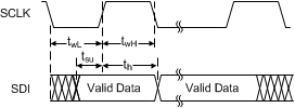 Figure 1. Write Timing Diagram
 Figure 2. Read Timing Diagram
7.8 Typical Characteristics
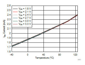
| Not including sensor current, default register settings. |

| Including sensor current. 13mm diameter sensor 0.1mm spacing/0.1mm trace width/ 4 layer 28 turns, fSENSOR = 2 MHz, RP_SET = 0x07, TX1=0x50, TC2=0x80, RCOUNT=0xFFFF, RESP_TIME =6144 |
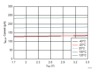
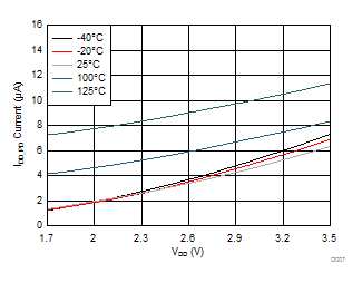

| RP_SET.RPMAX = b000 |
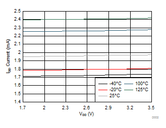
| Not including sensor current, default register settings. |
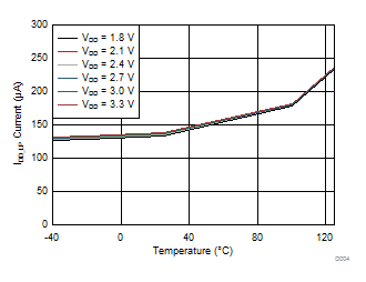
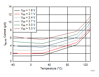

| RP_SET.RPMIN = b111 |