ZHCSJN1C September 2000 – September 2022 INA118
PRODUCTION DATA
- 1 特性
- 2 應(yīng)用
- 3 說明
- 4 Revision History
- 5 Device Comparison Table
- 6 Pin Configuration and Functions
- 7 Specifications
- 8 Detailed Description
- 9 應(yīng)用和實(shí)現(xiàn)
- 10Device and Documentation Support
- 11Mechanical, Packaging, and Orderable Information
封裝選項(xiàng)
機(jī)械數(shù)據(jù) (封裝 | 引腳)
散熱焊盤機(jī)械數(shù)據(jù) (封裝 | 引腳)
訂購信息
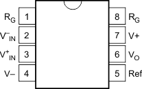
6 Pin Configuration and Functions
 Figure 6-1 P (8-Pin PDIP) and D (8-Pin
SOIC) Packages, Top View
Figure 6-1 P (8-Pin PDIP) and D (8-Pin
SOIC) Packages, Top ViewTable 6-1 Pin Functions
| PIN | TYPE | DESCRIPTION | |
|---|---|---|---|
| NO. | NAME | ||
| 1 | RG | — | Gain setting pin. For gains greater than 1, place a gain resistor between pin 1 and pin 8. |
| 2 | V–IN | Input | Negative input |
| 3 | V+IN | Input | Positive input |
| 4 | V– | Power | Negative supply |
| 5 | Ref | Input | Reference input. This pin must be driven by low impedance or connected to ground. |
| 6 | VO | Output | Output |
| 7 | V+ | Power | Positive supply |
| 8 | RG | — | Gain setting pin. For gains greater than 1, place a gain resistor between pin 1 and pin 8. |