ZHCSD97D January 2012 – January 2015 DS100BR111A
PRODUCTION DATA.
- 1 特性
- 2 應用
- 3 說明
- 4 簡化電路原理圖
- 5 修訂歷史記錄
- 6 Pin Configuration and Functions
- 7 Specifications
- 8 Detailed Description
- 9 Application and Implementation
- 10Power Supply Recommendations
- 11Layout
- 12器件和文檔支持
- 13機械封裝和可訂購信息
7 Specifications
7.1 Absolute Maximum Ratings(1)(2)
| MIN | MAX | UNIT | ||
|---|---|---|---|---|
| Supply Voltage (VDD) | -0.5 | 2.75 | V | |
| Supply Voltage (VIN) | -0.5 | 4.0 | V | |
| LVCMOS Input/Output Voltage | -0.5 | 4.0 | V | |
| CML Input Voltage | -0.5 | (VDD+0.5) | V | |
| CML Input Current | -30 | 30 | mA | |
| Junction Temperature | 125 | °C | ||
| Storage Temperature Range Tstg | -40 | 125 | °C | |
(1) “Absolute Maximum Ratings” indicate limits beyond which damage to the device may occur, including inoperability and degradation of device reliability and/or performance. Functional operation of the device and/or non-degradation at the Absolute Maximum Ratings or other conditions beyond those indicated in the Recommended Operating Conditions is not implied.
(2) For soldering specifications, see SNOA549.
7.2 ESD Ratings
| VALUE | UNIT | |||
|---|---|---|---|---|
| V(ESD) | Electrostatic discharge | Human-body model (HBM), per ANSI/ESDA/JEDEC JS-001(1) | ±5000 | V |
| Charged-device model (CDM), per JEDEC specification JESD22-C101(2) | ±1250 | |||
(1) JEDEC document JEP155 states that 500-V HBM allows safe manufacturing with a standard ESD control process.
(2) JEDEC document JEP157 states that 250-V CDM allows safe manufacturing with a standard ESD control process.
7.3 Recommended Operating Conditions(1)
| MIN | NOM | MAX | UNIT | |
|---|---|---|---|---|
| Supply Voltage (2.5 V mode) | 2.375 | 2.5 | 2.625 | V |
| Supply Voltage (3.3 V mode) | 3.0 | 3.3 | 3.6 | V |
| Ambient Temperature | -40 | 25 | +85 | °C |
| SMBus (SDA, SCL) | 3.6 | V |
(1) The Recommended Operating Conditions indicate conditions at which the device is functional and the device should not be operated beyond such conditions. Absolute Maximum Numbers are guaranteed for a junction temperature range of -40°C to +125°C. Models are validated to Maximum Operating Voltages only.
7.4 Thermal Information
| THERMAL METRIC(1) | DS100BR111A | UNIT | |
|---|---|---|---|
| WQFN/RTW | |||
| 24 PINS | |||
| RθJA | Junction-to-ambient thermal resistance, No Airflow, 4 layer JEDEC | 33 | °C/W |
| RθJC(top) | Junction-to-case (top) thermal resistance | 3.2 | |
(1) For more information about traditional and new thermal metrics, see the IC Package Thermal Metrics application report, SPRA953.
7.5 Electrical Characteristics
| PARAMETER | TEST CONDITIONS | MIN | TYP | MAX | UNIT | |
|---|---|---|---|---|---|---|
| POWER SUPPLY CURRENT | ||||||
| IDD | Supply Current | TX_DIS = Low, EQ = ON VOD_SEL = Float (850 mVpp) |
50 | 63 | mA | |
| Auto Low Power Mode TX_DIS = Low, MODE = 20 kΩ VID CHA and CHB = 0.0 V VOD_SEL = Float (850 mVpp) |
12 | 15 | ||||
| TX_DIS = HIGH | 25 | 35 | ||||
| LVCMOS DC SPECIFICATIONS | ||||||
| VIH25 | High Level Input Voltage, 2-Level LVCMOS |
2.5 V Supply Mode | 2.0 | VDD | V | |
| VIH33 | High Level Input Voltage, 2-Level LVCMOS |
3.3 V Supply Mode | 2.0 | VIN | V | |
| VIL | Low Level Input Voltage, 2-Level LVCMOS |
GND | 0.7 | V | ||
| VOH | High Level Output Voltage | IOH = -4.0 mA (3) | 2.0 | V | ||
| VOL | Low Level Output Voltage | IOL = 4.0 mA | 0.4 | V | ||
| IIN | Input Leakage Current | Vinput = 0 V or VDD VDD_SEL = Float |
-15 | 15 | µA | |
| Vinput = 0 V or VIN VDD_SEL = Low |
-15 | 15 | ||||
| IIN-P | Input Leakage Current 4-Level Input (1) |
Vinput = 0 V or VDD - 0.05 V VDD_SEL = Float Vinput = 0 V or VIN - 0.05 V VDD_SEL = Low |
-160 | 80 | µA | |
| CML RECEIVER INPUTS | ||||||
| VTX | Source Transmit Launch Differential Signal Level | Default power-up conditions ENSMB = 0 or 1 |
190 | 800 | 1600 | mVp-p |
| RLRX-IN | RX return loss | SDD11 @ 4.1 GHz | -12 | dB | ||
| SDD11 @ 11.1 GHz | -8 | |||||
| SCD11 @ 11.1 GHz | -10 | |||||
| HIGH SPEED TRANSMITTER OUTPUTS | ||||||
| VOD1 | Output Voltage Differential Swing | OUT+ and OUT- AC coupled and terminated by 50 Ω to GND VOD_SEL = Low (575 mVpp setting) DE = Low |
425 | 575 | 725 | mVp-p |
| VOD2 | Output Voltage Differential Swing | OUT+ and OUT- AC coupled and terminated by 50 Ω to GND VOD_SEL = Float (850 mVpp setting) DE = Low |
675 | 850 | 1025 | |
| VOD3 | Output Voltage Differential Swing | OUT+ and OUT- AC coupled and terminated by 50 Ω to GND VOD_SEL = 20 kΩ to GND (1050 mVpp) DE = Low |
850 | 1050 | 1275 | |
| VOD_DE1 | De-Emphasis Levels | OUT+ and OUT- AC coupled and terminated by 50 Ω to GND VOD_SEL = Float (850 mVpp) DE = Float |
-3.5 | dB | ||
| VOD_DE2 | De-Emphasis Levels | OUT+ and OUT- AC coupled and terminated by 50 Ω to GND VOD_SEL = Float (850 mVpp) DE = 20 kΩ to GND |
-6 | dB | ||
| VOD_DE3 | De-Emphasis Levels | OUT+ and OUT- AC coupled and terminated by 50 Ω to GND VOD_SEL = Float (850 mVpp) DE = HIGH |
-9 | dB | ||
| VCM-AC | Output Common-Mode Voltage | AC Common Mode Voltage DE = 0 dB, VOD ≤ 1000 mVpp |
4.5 | mV (rms) | ||
| VCM-DC | Output DC Common-Mode Voltage | DC Common Mode Voltage | 0 | 1.1 | 1.9 | V |
| VIDLE | TX IDLE Output Voltage | VID = 0 mVp-p | 30 | mV | ||
| RLTX-DIFF | TX return loss | SDD22 @ 4.1 GHz | -13 | dB | ||
| SDD22 @ 11.1 GHz | -9 | |||||
| SCC22 @ 2.5 GHz | -22 | |||||
| SCC22 @ 11.1 GHz | -10 | |||||
| Delta_ZM | Transmitter Termination Mismatch | DC, IFORCE = ± 100 µA (4) | 2.5% | |||
| TR/F | Transmitter Rise and Fall Time | Measurement points at 20% - 80% (7) | 38 | ps | ||
| TPD | Propagation Delay | Measured at 50% crossing EQ = 0x00 |
230 | ps | ||
| TCCSK | Channel to Channel Skew | T = 25°C, VDD = 2.5 V | 7 | ps | ||
| TPPSK | Part to Part Skew | T = 25°C, VDD = 2.5 V | 20 | ps | ||
| TTX-IDLE-SET-TO-IDLE | Max time to transition to idle after differential signal | VIN = 1 Vpp, 10 Gbps EQ = 0x00, DE = 0 dB |
6.5 | ns | ||
| TTX-IDLE-TO-DIFF-DATA | Max time to transition to valid differential signal after idle | VIN = 1 Vpp, 10 Gbps EQ = 0x00, DE = 0 dB |
3.2 | ns | ||
| TENV_DISTORT | Active OOB timing distortion, input active time vs. output active time | 3.3 | ns | |||
| OUTPUT JITTER SPECIFICATIONS(2) | ||||||
| RJ | Random Jitter | No Media Source Amplitude = 700 mVpp, PRBS15 pattern, 10.3125 Gbps VOD = Default, EQ = minimum, DE = 0 dB |
0.3 | ps (rms) | ||
| DJ1 | Deterministic Jitter | 0.09 | UI | |||
| EQUALIZATION | ||||||
| DJE1 | Residual Deterministic Jitter | 10.3125 Gbps 8 meter 30AWG Cable on Input Source = 700 mVpp, PRBS15 pattern EQ = 0x2B |
0.23 | UI | ||
| DJE2 | Residual Deterministic Jitter | 10.3125 Gbps 30" 4-mil FR4 on Inputs Source = 700 mVpp, PRBS15 pattern EQ = 0x17 |
0.15 | UI | ||
| DE-EMPHASIS | ||||||
| DJD1 | Residual Deterministic Jitter | 10.3125 Gbps 10” 4 mil stripline FR4 on Outputs Source = 700 mVpp, PRBS15 pattern EQ = Min, VOD = 1050 mVpp, DE = -3.5 dB |
0.14 | UI | ||
(1) Input is held to a maximum of 50 mV below VDD or VIN to simulate the use of a 1 kΩ resistor on the input.
(2) Typical jitter reported is determined by jitter decomposition software on the DSA8200 Oscilloscope.
(3) VOH only applies to the DONE pin; LOS, SCL, and SDA are open-drain outputs that have no internal pull-up capability. DONE is a full LVCMOS output with pull-up and pull-down capability.
(4) Force ±100 µA on output, measure ΔV on the Output and calculate impedance. Mismatch is the percentage difference of OUTn+ and OUTn- impedance driving the same logic state.
(5) Parameter not tested in production.
7.6 Electrical Characteristics — Serial Management Bus Interface
Over recommended operating supply and temperature ranges unless other specified.| PARAMETER | TEST CONDITIONS | MIN | TYP | MAX | UNIT | |
|---|---|---|---|---|---|---|
| SERIAL BUS INTERFACE DC SPECIFICATIONS(1) | ||||||
| VIL | Data, Clock Input Low Voltage | 0.8 | V | |||
| VIH | Data, Clock Input High Voltage | 2.1 | 3.6 | V | ||
| IPULLUP | Current Through Pull-Up Resistor or Current Source | High Power Specification | 4 | mA | ||
| VDD | Nominal Bus Voltage | 2.375 | 3.6 | V | ||
| ILEAK-Bus | Input Leakage Per Bus Segment | See (2) | -200 | 200 | µA | |
| CI | Capacitance for SDA and SCL | See (2)(3)(6) | 10 | pF | ||
| RTERM | External Termination Resistance pull to VDD = 2.5V ± 5% OR 3.3V ± 10% | Pullup VDD = 3.3 V, See (2)(3)(4) | 2000 | Ω | ||
| Pullup VDD = 2.5 V, See (2)(3)(4) | 1000 | Ω | ||||
| SERIAL BUS INTERFACE TIMING SPECIFICATIONS | ||||||
| FSMB | Bus Operating Frequency | ENSMB = VDD (Slave Mode) | 400 | kHz | ||
| ENSMB = Float (Master Mode) (1) | 280 | 400 | 520 | kHz | ||
| TBUF | Bus Free Time Between Stop and Start Condition | 1.3 | µs | |||
| THD:STA | Hold time after (Repeated) Start Condition. After this period, the first clock is generated. | At IPULLUP, Max | 0.6 | µs | ||
| TSU:STA | Repeated Start Condition Setup Time | 0.6 | µs | |||
| TSU:STO | Stop Condition Setup Time | 0.6 | µs | |||
| THD:DAT | Data Hold Time | 0 | ns | |||
| TSU:DAT | Data Setup Time | 100 | ns | |||
| TLOW | Clock Low Period | 1.3 | µs | |||
| THIGH | Clock High Period | See (5) | 0.6 | 50 | µs | |
| tF | Clock/Data Fall Time | See (5) | 300 | ns | ||
| tR | Clock/Data Rise Time | See (5) | 300 | ns | ||
| tPOR | Time in which a device must be operational after power-on reset | See (6)(5) | 500 | ms | ||
(1) EEPROM interface requires 1 MHz capable EEPROM device.
(2) Recommended value.
(3) Recommended maximum capacitance load per bus segment is 400 pF.
(4) Maximum termination voltage should be identical to the device supply voltage.
(5) Compliant to SMBus 2.0 physical layer specification. See System Management Bus (SMBus) Specification Version 2.0, section 3.1.1 SMBus common AC specifications for details.
(6) Guaranteed by design and characterization. Parameter not tested in production.
(7) Default VOD used for testing. DE = -1.5 dB level used to compensate for fixture attenuation.
7.7 Timing Requirements — LOS and ENABLE / DISABLE Timing
| MIN | NOM | MAX | UNIT | |||
|---|---|---|---|---|---|---|
| TLOS_OFF | Input IDLE to Active RX_LOS response time |
See (5) | 0.035 | µs | ||
| TLOS_ON | Input Active to IDLE RX_LOS response time |
See (5) | 0.4 | µs | ||
| TOFF | TX Disable assert Time TX_DIS = HIGH to Output OFF |
See (5) | 0.005 | µs | ||
| TON | TX Disable negateTime TX_DIS = Low to Output ON |
See (5) | 0.150 | µs | ||
| TLP_EXIT | Auto Low Power Exit ALP to Normal Operation |
See (5) | 150 | ns | ||
| TLP_ENTER | Auto Low Power Enter Normal Operation to Auto Low Power |
See (5) | 100 | µs |
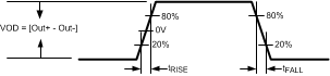 Figure 1. Output Rise and Fall Transition Times
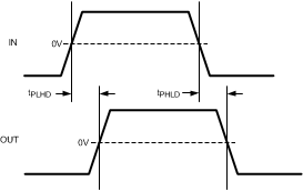 Figure 2. Propagation Delay Timing Diagram
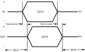 Figure 3. Transmit Idle-Data and Data-Idle Response Time
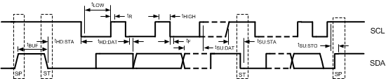 Figure 4. SMBus Timing Parameters
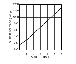
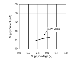
7.8 Typical Characteristics
The following data was collected at 25°C.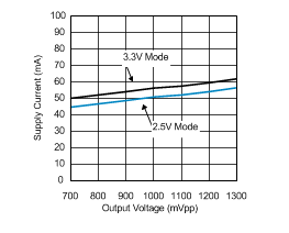
| VOD = 575 mVpp |