ZHCS138C August 2011 – March 2016 DRV8302
PRODUCTION DATA.
- 1 特性
- 2 應(yīng)用范圍
- 3 說明
- 4 修訂歷史記錄
- 5 Pin Configuration and Functions
- 6 Specifications
- 7 Detailed Description
- 8 Application and Implementation
- 9 Power Supply Recommendations
- 10Layout
- 11器件和文檔支持
- 12機(jī)械、封裝和可訂購信息
封裝選項(xiàng)
機(jī)械數(shù)據(jù) (封裝 | 引腳)
- DCA|56
散熱焊盤機(jī)械數(shù)據(jù) (封裝 | 引腳)
- DCA|56
訂購信息
6 Specifications
6.1 Absolute Maximum Ratings
over operating free-air temperature range (unless otherwise noted)(1)(1) Stresses beyond those listed under Absolute Maximum Ratings may cause permanent damage to the device. These are stress ratings only, which do not imply functional operation of the device at these or any other conditions beyond those indicated under Recommended Operating Conditions. Exposure to absolute-maximum-rated conditions for extended periods may affect device reliability.
6.2 ESD Ratings
| VALUE | UNIT | |||
|---|---|---|---|---|
| V(ESD) | Electrostatic discharge | Human-body model (HBM), per ANSI/ESDA/JEDEC JS-001(1) | ±2000 | V |
| Charged-device model (CDM), per JEDEC specification JESD22-C101(2) | ±500 | |||
(1) JEDEC document JEP155 states that 500-V HBM allows safe manufacturing with a standard ESD control process.
(2) JEDEC document JEP157 states that 250-V CDM allows safe manufacturing with a standard ESD control process.
6.3 Recommended Operating Conditions
| MIN | NOM | MAX | UNIT | |||
|---|---|---|---|---|---|---|
| VPVDD | DC supply voltage PVDD1 for normal operation | Relative to PGND | 8 | 60 | V | |
| DC supply voltage PVDD2 for buck converter | 3.5 | 60 | V | |||
| IDIN_EN | Input current of digital pins when EN_GATE is high | 100 | µA | |||
| IDIN_DIS | Input current of digital pins when EN_GATE is low | 1 | µA | |||
| CO_OPA | Maximum output capacitance on outputs of shunt amplifier | 20 | pF | |||
| RDTC | Dead time control resistor range. Time range is 50 ns (–GND) to 500 ns (150 kΩ) with a linear approximation. | 0 | 150 | kΩ | ||
| IFAULT | FAULT pin sink current. Open drain | V = 0.4 V | 2 | mA | ||
| IOCTW | OCTW pin sink current. Open drain | V = 0.4 V | 2 | mA | ||
| VREF | External voltage reference voltage for current shunt amplifiers | 2 | 6 | V | ||
| fgate | Operating switching frequency of gate driver | Qg(TOT) = 25 nC or total 30-mA gate drive average current | 200 | kHz | ||
| TA | Ambient temperature | –40 | 125 | °C | ||
6.4 Thermal Information
| THERMAL METRIC(1) | DRV8302 | UNIT | |
|---|---|---|---|
| DCA (HTSSOP) | |||
| 56 PINS | |||
| RθJA | Junction-to-ambient thermal resistance | 30.3 | °C/W |
| RθJC(top) | Junction-to-case (top) thermal resistance | 33.5 | °C/W |
| RθJB | Junction-to-board thermal resistance | 17.5 | °C/W |
| ψJT | Junction-to-top characterization parameter | 0.9 | °C/W |
| ψJB | Junction-to-board characterization parameter | 7.2 | °C/W |
| RθJC(bot) | Junction-to-case (bottom) thermal resistance | 0.9 | °C/W |
(1) For more information about traditional and new thermal metrics, see the Semiconductor and IC Package Thermal Metrics application report (SPRA953).
6.5 Electrical Characteristics
PVDD = 8 V to 60 V, TC = 25°C, unless specified under test condition6.6 Gate Timing and Protection Characteristics
| MIN | NOM | MAX | UNIT | |||
|---|---|---|---|---|---|---|
| TIMING, OUTPUT PINS | ||||||
| tpd,If-O | Positive input falling to GH_x falling | CL=1 nF, 50% to 50% | 45 | ns | ||
| tpd,Ir-O | Positive input rising to GL_x falling | CL=1 nF, 50% to 50% | 45 | ns | ||
| Td_min | Minimum dead time after hand shaking(1) | 50 | ns | |||
| Tdtp | Dead Time | With RDTC set to different values | 50 | 500 | ns | |
| tGDr | Rise time, gate drive output | CL=1 nF, 10% to 90% | 25 | ns | ||
| tGDF | Fall time, gate drive output | CL=1 nF, 90% to 10% | 25 | ns | ||
| TON_MIN | Minimum on pulse | Not including handshake communication. Hiz to on state, output of gate driver | 50 | ns | ||
| Tpd_match | Propagation delay matching between high side and low side | 5 | ns | |||
| Tdt_match | Deadtime matching | 5 | ns | |||
| TIMING, PROTECTION AND CONTROL | ||||||
| tpd,R_GATE-OP | Start-up time, from EN_GATE active high to device ready for normal operation | PVDD is up before start-up, all charge pump caps and regulator caps as in recommended condition | 5 | 10 | ms | |
| tpd,R_GATE-Quick | If EN_GATE goes from high to low and back to high state within quick reset time, it will only reset all faults and gate driver without powering down charge pump, current amp, and related internal voltage regulators. | Maximum low pulse time | 10 | us | ||
| tpd,E-L | Delay, error event to all gates low | 200 | ns | |||
| tpd,E-FAULT | Delay, error event to FAULT low | 200 | ns | |||
| OTW_CLR | Junction temperature for resetting overtemperature warning | 115 | °C | |||
| OTW_SET/OTSD_CLR | Junction temperature for overtemperature warning and resetting overtemperature shut down | 130 | °C | |||
| OTSD_SET | Junction temperature for overtemperature shut down | 150 | °C | |||
(1) Dead time programming definition: Adjustable delay from GH_x falling edge to GL_X rising edge, and GL_X falling edge to GH_X rising edge. This is a minimum dead-time insertion. It is not added to the value set by the microcontroller externally.
6.7 Current Shunt Amplifier Characteristics
TC = 25°C unless otherwise specified| PARAMETER | TEST CONDITIONS | MIN | TYP | MAX | UNIT | |
|---|---|---|---|---|---|---|
| G1 | Gain option 1 | (GAIN = 0 V) | 9.5 | 10 | 10.5 | V/V |
| G2 | Gain option 2 | (GAIN = 2 V) | 38 | 40 | 42 | V/V |
| Tsettling | Settling time to 1% | Tc = 0°C to 60°C, G = 10, Vstep = 2 V | 300 | ns | ||
| Tsettling | Settling time to 1% | Tc = 0°C to 60°C, G = 40, Vstep = 2 V | 1.2 | µs | ||
| Vswing | Output swing linear range | 0.3 | 5.7 | V | ||
| Slew Rate | G = 10 | 10 | V/µs | |||
| DC_offset | Offset error RTI | G = 10 with input shorted | 4 | mV | ||
| Drift_offset | Offset drift RTI | 10 | µV/C | |||
| Ibias | Input bias current | 100 | µA | |||
| Vin_com | Common input mode range | –0.15 | 0.15 | V | ||
| Vin_dif | Differential input range | –0.3 | 0.3 | V | ||
| Vo_bias | Output bias | With zero input current, Vref up to 6 V | –0.5% | 0.5×Vref | 0.5% | V |
| CMRR_OV | Overall CMRR with gain resistor mismatch | CMRR at DC, gain = 10 | 70 | 85 | dB | |
6.8 Buck Converter Characteristics
TC = 25°C unless otherwise specified6.9 Typical Characteristics

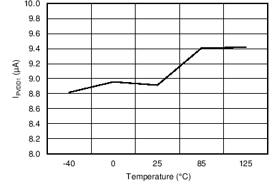
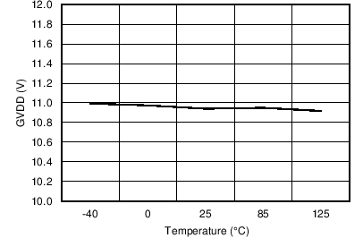
(PVDD1 = 8 V, EN_GATE = LOW)


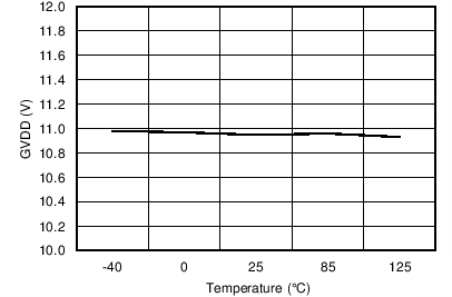
(PVDD1 = 8 V, EN_GATE = HIGH)