| STATIC CHARACTERISTICS |
| BVDSS |
Drain-to-Source Voltage |
VGS = 0 V, ID = –250 μA |
–12 |
|
|
V |
| BVGSS |
Gate-to-Source Voltage; |
VDS = 0 V, IG = –250 μA |
–6 |
|
–7.2 |
V |
| IDSS |
Drain-to-Source Leakage Current |
VGS = 0 V, VDS = –9.6 V |
|
|
–1 |
μA |
| IGSS |
Gate-to-Source Leakage Current |
VDS = 0 V, VGS = –6 V |
|
|
–100 |
nA |
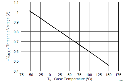
| VGS(th) |
Gate-to-Source Threshold Voltage |
VDS = VGS, ID = –250 μA |
–0.4 |
–0.6 |
–0.9 |
V |
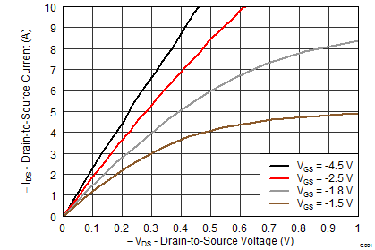
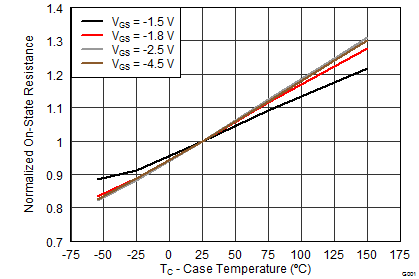
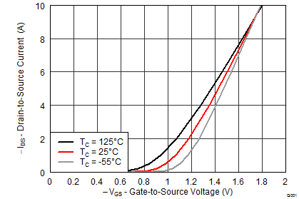
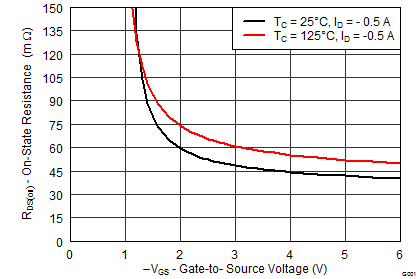
| RDS(on) |
Drain-to-Source On-Resistance |
VGS = –1.5 V, ID = –0.5 A |
|
82 |
123 |
mΩ |
| VGS = –1.8 V, ID = –0.5 A |
|
67 |
92 |
mΩ |
| VGS = –2.5 V, ID = –0.5 A |
|
54 |
66 |
mΩ |
| VGS = –4.5 V, ID = –0.5 A |
|
44 |
53 |
mΩ |
| gƒs |
Transconductance |
VDS = –1.2 V, ID = –0.5 A |
|
5.6 |
|
S |
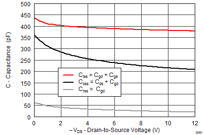
| DYNAMIC CHARACTERISTICS |
| CISS |
Input Capacitance |
VGS = 0 V, VDS = –6.0 V, ƒ = 1 MHz |
|
394 |
512 |
pF |
| COSS |
Output Capacitance |
|
238 |
310 |
pF |
| CRSS |
Reverse Transfer Capacitance |
|
29 |
37 |
pF |
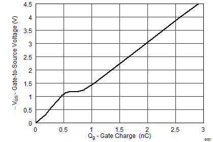
| Qg |
Gate Charge Total (–4.5 V) |
VDS = –6 V, ID = –0.5 A |
|
2.9 |
3.8 |
nC |
| Qgd |
Gate Charge Gate-to-Drain |
|
0.28 |
|
nC |
| Qgs |
Gate Charge Gate-to-Source |
|
0.55 |
|
nC |
| Qg(th) |
Gate Charge at Vth |
|
0.29 |
|
nC |
| QOSS |
Output Charge |
VDS = –6 V, VGS = 0 V |
|
2.0 |
|
nC |
| td(on) |
Turn On Delay Time |
VDS = –6 V, VGS = –4.5 V,
ID = –0.5 A RG = 0 Ω |
|
9 |
|
ns |
| tr |
Rise Time |
|
4 |
|
ns |
| td(off) |
Turn Off Delay Time |
|
58 |
|
ns |
| tƒ |
Fall Time |
|
21 |
|
ns |
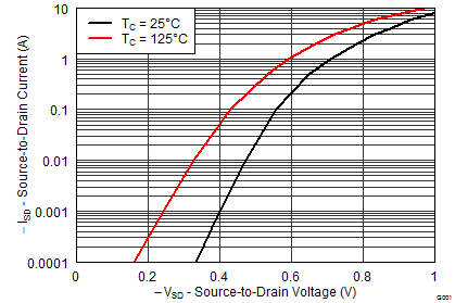
| DIODE CHARACTERISTICS |
| VSD |
Diode Forward Voltage |
IS = –0.5 A, VGS = 0 V |
|
–0.66 |
–1 |
V |
| Qrr |
Reverse Recovery Charge |
VDS= –6 V, IF = –0.5 A, di/dt = 100 A/μs |
|
3.7 |
|
nC |
| trr |
Reverse Recovery Time |
|
12 |
|
ns |