SLUS891B February 2010 – November 2014
PRODUCTION DATA.
- 1 Features
- 2 Applications
- 3 Description
- 4 Revision History
- 5 Pin Configuration and Functions
- 6 Specifications
-
7 Detailed Description
- 7.1 Overview
- 7.2 Functional Block Diagram
- 7.3
Feature Description
- 7.3.1 Battery Voltage Regulation
- 7.3.2 Battery Current Regulation
- 7.3.3 Precharge
- 7.3.4 Charge Termination, Recharge, and Safety Timer
- 7.3.5 Power Up
- 7.3.6 Enable and Disable Charging
- 7.3.7 Automatic Internal Soft-Start Charger Current
- 7.3.8 Cycle-by-Cycle Charge Undercurrent Protection
- 7.3.9 Input Overvoltage Protection (ACOV)
- 7.3.10 Input Undervoltage Lock-Out (UVLO)
- 7.3.11 Battery Overvoltage Protection
- 7.3.12 Cycle-by-Cycle Charge Overcurrent Protection
- 7.3.13 Thermal Shutdown Protection
- 7.3.14 Temperature Qualification
- 7.3.15 Timer Fault Recovery
- 7.3.16 PG Output
- 7.3.17 CE (Charge Enable)
- 7.3.18 Inductor, Capacitor, and Sense Resistor Selection Guidelines
- 7.3.19 Charge Status Outputs
- 7.3.20 Battery Detection
- 7.4 Device Functional Modes
- 7.5 Application Information
- 7.6 Typical Application
- 8 Power Supply Recommendations
- 9 Layout
- 10Device and Documentation Support
- 11Mechanical, Packaging, and Orderable Information
封裝選項
機械數(shù)據(jù) (封裝 | 引腳)
- RVA|16
散熱焊盤機械數(shù)據(jù) (封裝 | 引腳)
- RVA|16
訂購信息
5 Pin Configuration and Functions
RVA Package
(Top View)
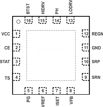
Pin Functions
| PIN | I/O | FUNCTION DESCRIPTION | |
|---|---|---|---|
| NAME | NO. | ||
| VCC | 1 | I | IC power positive supply. Connect, through a 10-Ω resistor to the common-source (diode-OR) point: source of high-side P-channel MOSFET and source of reverse-blocking power P-channel MOSFET. Or connect through a 10-Ω resistor to the cathode of the input diode. Place a 1-μF ceramic capacitor from VCC to the GND pin close to the IC. |
| CE | 2 | I | Charge-enable active-HIGH logic input. HI enables charge. LO disables charge. It has an internal 1MΩ pull-down resistor. |
| STAT | 3 | I | Open-drain charge status pin to indicate various charger operation (See Table 2) |
| TS | 4 | I | Temperature qualification voltage input for battery pack negative temperature coefficient thermistor. Program the hot and cold temperature window with a resistor divider from VREF to TS to GND. |
| PG | 5 | O | Open-drain power-good status output. The transistor turns on when a valid VCC is detected. It is turned off in the sleep mode. PG can be used to drive an LED or communicate with a host processor. It can be used to drive ACFET and BATFET. |
| VREF | 6 | O | 3.3-V regulated voltage output. Place a 1-μF ceramic capacitor from VREF to the GND pin close to the IC. This voltage could be used for programming of voltage and current regulation and for programming the TS threshold. |
| ISET | 7 | I | Charge current set input. The voltage of ISET pin programs the charge current regulation, pre-charge current and termination current set-point. |
| VFB | 8 | O | Output voltage analog feedback adjustment. Connect the output of a resistive voltage divider from the battery terminals to this node to adjust the output battery regulation voltage. |
| SRN | 9 | I | Charge-current sense resistor, negative input. A 0.1-μF ceramic capacitor is placed from SRN to SRP to provide differential-mode filtering. An optional 0.1-μF ceramic capacitor is placed from SRN pin to GND for common-mode filtering. |
| SRP | 10 | I | Charge-current sense resistor, positive input. A 0.1-μF ceramic capacitor is placed from SRN to SRP to provide differential-mode filtering. A 0.1-μF ceramic capacitor is placed from SRP pin to GND for common-mode filtering. |
| GND | 11 | -- | Low-current sensitive analog/digital ground. On PCB layout, connect with thermal pad underneath the IC. |
| REGN | 12 | O | PWM low-side driver positive 6-V supply output. Connect a 1-μF ceramic capacitor from REGN to the PGND pin, close to the IC. Use for low-side driver and high-side driver bootstrap voltage by connecting a small-signal Schottky diode from REGN to BTST. |
| LODRV | 13 | O | PWM low-side driver output. Connect to the gate of the low-side power MOSFET with a short trace. |
| PH | 14 | I | PWM high-side driver negative supply. Connect to the phase-switching node (junction of the low-side power MOSFET drain, high-side power MOSFET source, and output inductor). |
| HIDRV | 15 | O | PWM high-side driver output. Connect to the gate of the high-side power MOSFET with a short trace. |
| BTST | 16 | I | PWM high-side driver negative supply. Connect the 0.1-μF bootstrap capacitor from PH to BTST, and a bootstrap Schottky diode from REGN to BTST. |
| Thermal pad | -- | -- | Exposed pad beneath the IC. Always solder thermal pad to the board, and have vias on the thermal pad plane star-connecting to GND and ground plane for high-current power converter. It also serves as a thermal pad to dissipate the heat. |