SLPS418A June 2013 – June 2014 CSD75207W15
PRODUCTION DATA.
- 1Features
- 2Applications
- 3Description
- 4Revision History
- 5Specifications
- 6Device and Documentation Support
- 7Mechanical, Packaging, and Orderable Information
Package Options
Refer to the PDF data sheet for device specific package drawings
Mechanical Data (Package|Pins)
- YZF|9
Thermal pad, mechanical data (Package|Pins)
Orderable Information
1 Features
- Dual P-Channel MOSFETs
- Common Source Configuration
- Small Footprint 1.5-mm × 1.5-mm
- Gate-Source Voltage Clamp
- Gate ESD Protection >4 kV
- HBM JEDEC standard JESD22-A114
- Pb and Halogen Free
- RoHS Compliant
2 Applications
- Battery Management
- Battery Protection
- Load and Input Switching
3 Description
The CSD75207W15 device is designed to deliver the lowest on-resistance and gate charge in the smallest outline possible with excellent thermal characteristics in an ultra-low profile. Low on-resistance coupled with the small footprint and low profile make the device ideal for battery-operated space-constrained applications. The device has also been awarded with U.S. patents 7952145, 7420247, 7235845, and 6600182.

Product Summary
| TA = 25°C | TYPICAL VALUE | UNIT | ||
|---|---|---|---|---|
| VD1D2 | Drain-to-Drain Voltage | –20 | V | |
| Qg | Gate Charge Total (–4.5 V) | 2.9 | nC | |
| Qgd | Gate Charge Gate to Drain | 0.4 | nC | |
| RD1D2(on) | Drain-to-Drain On Resistance | VGS = –1.8 V | 119 | mΩ |
| VGS = –2.5 V | 64 | mΩ | ||
| VGS = –4.5 V | 45 | mΩ | ||
| VGS(th) | Threshold Voltage | –0.8 | V | |
Ordering Information(1)
| Device | Package | Media | Qty | Ship |
|---|---|---|---|---|
| CSD75207W15 | 1.5-mm × 1.5-mm Wafer Level Package | 7-Inch Reel | 3000 | Tape and Reel |
- For all available packages, see the orderable addendum at the end of the data sheet.
Absolute Maximum Ratings
| TA = 25°C | VALUE | UNIT | |
|---|---|---|---|
| VD1D2 | Drain-to-Drain Voltage | –20 | V |
| VGS | Gate-to-Source Voltage | –6.0 | V |
| ID1D2 | Continuous Drain to Drain Current(1)(2) | –3.9 | A |
| Pulsed Drain to Drain Current, TC = 25°C(3) |
–24 | A | |
| IS | Continuous Source Pin Current | –1.2 | A |
| Pulsed Source Pin Current(3) | –15 | A | |
| IG | Continuous Gate Clamp Current | –0.5 | A |
| Pulsed Gate Clamp Current(3) | –7 | A | |
| PD | Power Dissipation(1) | 0.7 | W |
| TJ, Tstg |
Operating Junction and Storage Temperature Range |
–55 to 150 | °C |
Top View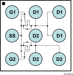 |
RD1D2(on) vs VGS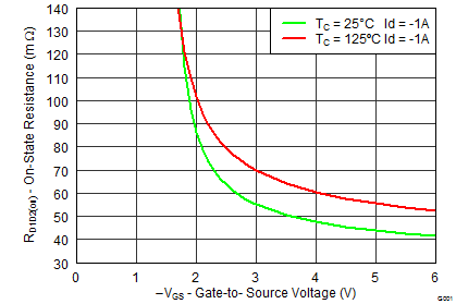 |