ZHCSCV6B August 2014 – January 2024 UCC27511A-Q1
PRODUCTION DATA
- 1
- 1 特性
- 2 應用
- 3 說明
- 4 Pin Configuration and Functions
- 5 Specifications
- 6 Detailed Description
- 7 Application and Implementation
- 8 Power Supply Recommendations
- 9 Layout
- 10Device and Documentation Support
- 11Revision History
- 12Mechanical, Packaging, and Orderable Information
5.6 Switching Characteristics
VDD = 12 V, TA = TJ = –40°C to 140°C, 1-μF capacitor from
VDD to GND. Currents are positive into, negative out of the
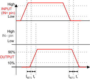
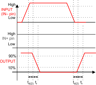
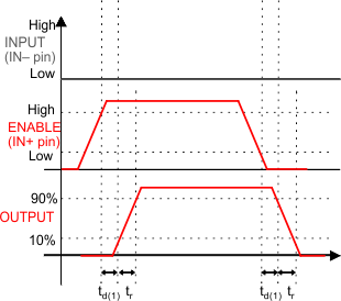
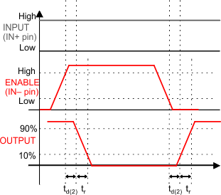
specified terminal. See Figure 5-1, Figure 5-2, Figure 5-3, and Figure 5-4
| PARAMETER | TEST CONDITIONS | MIN | TYP | MAX | UNIT | |
|---|---|---|---|---|---|---|
| tr | Rise time(1) | VDD = 12 V C(LOAD) = 1.8 nF, connected to OUTH and OUTL pins tied together | 8 | 12 | ns | |
| VDD = 4.5 V C(LOAD) = 1.8 nF | 16 | 22 | ||||
| tf | Fall time(1) | VDD = 12 V C(LOAD) = 1.8 nF, connected to OUTH and OUTL pins tied together | 7 | 11 | ns | |
| VDD = 4.5 V C(LOAD) = 1.8 nF | 7 | 11 | ||||
| td(1) | IN+ to output propagation delay(1) | VDD = 12 V 5-V input pulse C(LOAD) = 1.8 nF, connected to OUTH and OUTL pins tied together | 4 | 13 | 23 | ns |
| VDD = 4.5 V 5-V input pulse C(LOAD) = 1.8 nF, connected to OUTH and OUTL pins tied together | 4 | 15 | 26 | |||
| td(2) | IN– to output propagation delay(1) | VDD = 12 V C(LOAD) = 1.8 nF, connected to OUTH and OUTL pins tied together | 4 | 13 | 23 | ns |
| VDD = 4.5 V C(LOAD) = 1.8 nF, connected to OUTH and OUTL pins tied together | 4 | 19 | 30 | |||
 Figure 5-1 Non-Inverting Configuration (PWM Input to IN+ pin (IN– Pin Tied to GND), Output Represents OUTH and OUTL Pins Tied Together in the UCC27511A-Q1)
 Figure 5-2 Inverting Configuration (PWM Input to IN– Pin (IN+ Pin Tied to VDD), Output Represents OUTH and OUTL Pins Tied Together in the UCC27511A-Q1)
 Figure 5-3 Enable And Disable Function Using IN+ Pin (Enable and Disable Signal Applied to IN+ Pin, PWM Input to IN– Pin, Output Represents OUTH and OUTL Pins Tied Together in the UCC27511A-Q1)
 Figure 5-4 Enable and Disable Function Using IN– Pin (Enable and Disable Signal Applied to IN– Pin, PWM Input to IN+ Pin, Output Represents OUTH and OUTL Pins Tied Together in the UCC27511A-Q1)