SLVS440C January 2003 – December 2014 TPS61045
PRODUCTION DATA.
- 1 Features
- 2 Applications
- 3 Description
- 4 Revision History
- 5 Pin Configuration and Functions
- 6 Specifications
- 7 Detailed Description
- 8 Application and Implementation
- 9 Power Supply Recommendations
- 10Layout
- 11Device and Documentation Support
- 12Mechanical, Packaging, and Orderable Information
封裝選項
請參考 PDF 數(shù)據(jù)表獲取器件具體的封裝圖。
機械數(shù)據(jù) (封裝 | 引腳)
- DRB|8
散熱焊盤機械數(shù)據(jù) (封裝 | 引腳)
- DRB|8
訂購信息
6 Specifications
6.1 Absolute Maximum Ratings
over operating free-air temperature (unless otherwise noted)(1)| MIN | MAX | UNIT | ||
|---|---|---|---|---|
| Supply voltage | VVIN(2) | –0.3 | 7 | V |
| Voltage | VCTRL, V(FB), VL, VDO(2) | –0.3 | VIN + 0.3 | V |
| Voltage | VSW(2) | 30 | V | |
| Continuous power dissipation | See Dissipation Rating | |||
| TJ | Operating junction temperature | –40 | 150 | °C |
| Tstg | Storage temperature | –65 | 150 | °C |
(1) Stresses beyond those listed under absolute maximum ratings may cause permanent damage to the device. These are stress ratings only, and functional operation of the device at these or any other conditions beyond those indicated under recommended operating conditions is not implied. Exposure to absolute-maximum-rated conditions for extended periods may affect device reliability.
(2) All voltage values are with respect to network ground pin.
6.2 ESD Ratings
| VALUE | UNIT | |||
|---|---|---|---|---|
| V(ESD) | Electrostatic discharge | Human body model (HBM), per ANSI/ESDA/JEDEC JS-001, all pins(1) | ±1500 | V |
| Charged device model (CDM), per JEDEC specification JESD22-C101, all pins(2) | ±500 | |||
(1) JEDEC document JEP155 states that 500-V HBM allows safe manufacturing with a standard ESD control process.
(2) JEDEC document JEP157 states that 250-V CDM allows safe manufacturing with a standard ESD control process.
6.3 Recommended Operating Conditions
| MIN | TYP | MAX | UNIT | ||
|---|---|---|---|---|---|
| VVIN | Input voltage range | 1.8 | 6 | V | |
| VSW | Switch voltage | 30 | V | ||
| L | Inductor (1) | 4.7 | μH | ||
| ƒ | Switching frequency(1) | 1 | MHz | ||
| CI(C2) | Input capacitor (C2) (1) | 4.7 | μF | ||
| CO(C3) | Output capacitor (C3) (1) | 1 | μF | ||
| TA | Operating ambient temperature | –40 | 85 | °C | |
| TJ | Operating junction temperature | –40 | 125 | °C | |
(1) See application section for further information.
6.4 Thermal Information
over operating free-air temperature range (unless otherwise noted)| THERMAL METRIC(1) | TPS61045 | UNIT | ||
|---|---|---|---|---|
| VSON (8 PINS) | ||||
| RΘJA(2) | Junction-to-ambient thermal resistance | 270 | °C/W | |
(1) For more information about traditional and new thermal metrics, see the IC Package Thermal Metrics application report, SPRA953.
(2) Standard 2-layer PCB without vias for the thermal pad. See the application section on how to improve the thermal resistance RΘJA.
6.5 Dissipation Rating
| PACKAGE | TA ≤ 25°C POWER RATING |
DERATING FACTOR ABOVE TA = 25°C | TA = 70°C POWER RATING |
TA = 85°C POWER RATING |
|---|---|---|---|---|
| 8-pin VSON (DRB) (1) | 370 mW | 3.7 mW/°C | 204 mW | 148 mW |
(1) See Thermal Information for the junction-to-ambient thermal resistance.
6.6 Electrical Characteristics
VIN = 2.4 V, CTRL = VIN, VO = 18 V, IO = 10 mA, TA = –40°C to 85°C, typical values are at TA = 25° C (unless otherwise noted)| PARAMETER | TEST CONDITIONS | MIN | TYP | MAX | UNIT | |
|---|---|---|---|---|---|---|
| SUPPLY CURRENT | ||||||
| VIN | Input voltage range | 1.8 | 6 | V | ||
| IQ | Operating quiescent current | IO = 0 mA, not switching | 40 | 65 | μA | |
| IO(SD) | Shutdown current | CTRL = GND | 0.1 | 1 | μA | |
| UVLO | Undervoltage lockout (UVLO) threshold | VIN falling | 1.5 | 1.7 | V | |
| CTRL AND DAC OUTPUT | ||||||
| VIH | CTRL high-level input voltage | 1.3 | V | |||
| VIL | CTRL low-level input voltage | 0.3 | V | |||
| Ilkg | CTRL input leakage current | CTRL = GND or VIN | 0.1 | μA | ||
| VO(DO) | DAC output voltage range | 0 | 1.233 | V | ||
| DAC resolution | 6 bit | 19.6 | mV | |||
| VO(DO) | DAC center output voltage | CTRL = high | 607 | mV | ||
| IO(SINK) | Maximum DAC sink current | 30 | μA | |||
| tUP | Increase output voltage one step | CTRL = High to low to high | 1 | 60 | μs | |
| tDWN | Decrease the output voltage one step | CTRL = High to low to high | 140 | 240 | μs | |
| td1 | Delay time between up and down steps | CTRL = Low to high to low | 1 | μs | ||
| tOFF | Shutdown | CTRL = High to low to high | 560 | μs | ||
| INPUT SWITCH (Q1), MAIN SWITCH (Q2), AND CURRENT LIMIT | ||||||
| VSW(Q2) | Main switch maximum voltage (Q2) | 30 | V | |||
| rDS(on) | Main switch MOSFET on-resistance | VIN = 2.4 V; IS = 200 mA | 400 | 800 | mΩ | |
| Ilkg | Main switch MOSFET leakage current | VS = 28 V | 0.1 | 10 | μA | |
| ILIM | Main switch MOSFET current limit | 300 | 375 | 450 | mA | |
| rDS(on) | Input switch MOSFET on-resistance | VIN = 2.4 V; IS = 200 mA | 1 | 2 | Ω | |
| Ilkg | Input switch MOSFET leakage current | VL = GND, VIN = 6 V | 0.1 | 10 | μA | |
| OUTPUT | ||||||
| VO | Output voltage range | VIN | 28 | V | ||
| Vref | Internal voltage reference | 1.233 | V | |||
| IFB | Feedback input bias current | V(FB) = 1.3 V | 30 | 100 | nA | |
| VFB | Feedback trip point voltage | 1.8 V ≤ VIN ≤ 6 V; VO = 18 V, ILOAD = 10 mA | 1.208 | 1.233 | 1.258 | V |
| Feedback trip point voltage | 1.8 V ≤ VIN≤ 3.6 V; VO = 18 V, ILOAD = 10 mA , TA = 0°C to 85°C |
1.214 | 1.233 | 1.251 | V | |
6.7 Typical Characteristics
Table 1. Table of Graphs
| Graph Title | Figure | |
|---|---|---|
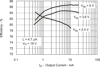
| η | Efficiency vs Load Current | Figure 1 |
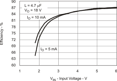
| Efficiency vs Input Voltage | Figure 2 | |
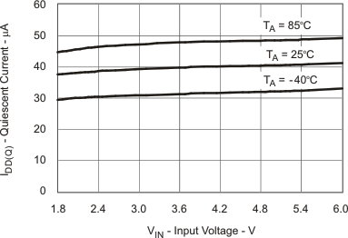
| IDD(Q) | Quiescent Current vs Input Voltage | Figure 3 |
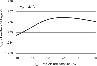
| VFB | Feedback Voltage vs Temperature | Figure 4 |
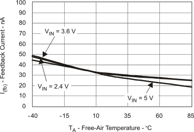
| IFB | Feedback Current vs Temperature | Figure 5 |
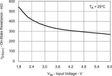
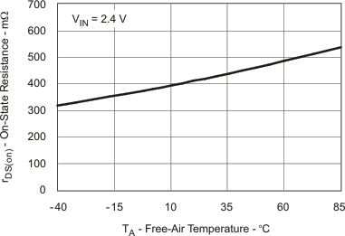
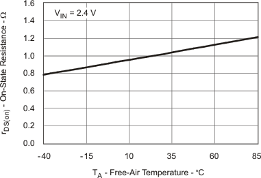
| rDS(on) | rDS(on) Main Switch Q2 vs Temperature | Figure 6 |
| rDS(on) Main Switch Q2 vs Input Voltage | Figure 7 | |
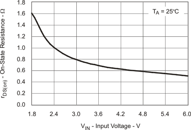
| rDS(on) Input Switch Q1 vs Temperature | Figure 8 | |
| rDS(on) Input Switch Q1 vs Input Voltage | Figure 9 | |
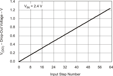
| VDO | VDO Voltage vs CTRL Input Step | Figure 10 |
| Line Transient Response | Figure 13 | |
| Load Transient Response | Figure 14 | |
| PFM Operation | Figure 15 | |
| Softstart | Figure 16 | |