ZHCSA62B August 2012 – August 2014 TPS22965
PRODUCTION DATA.
- 1 特性
- 2 應(yīng)用范圍
- 3 說明
- 4 簡化電路原理圖
- 5 修訂歷史記錄
- 6 Pin Configuration and Functions
- 7 Specifications
- 8 Detailed Description
- 9 Application and Implementation
- 10Power Supply Recommendations
- 11Layout
- 12器件和文檔支持
- 13機械封裝和可訂購信息
封裝選項
機械數(shù)據(jù) (封裝 | 引腳)
- DSG|8
散熱焊盤機械數(shù)據(jù) (封裝 | 引腳)
- DSG|8
訂購信息
6 Pin Configuration and Functions
DSG PACKAGE
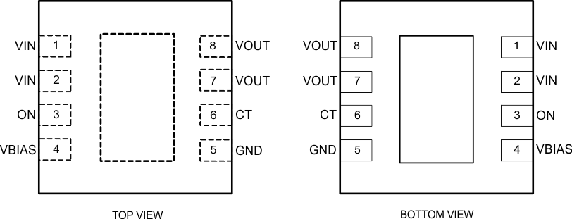
Pin Functions
| PIN | I/O | DESCRIPTION | |
|---|---|---|---|
| NAME | DSG | ||
| CT | 6 | O | Switch slew rate control. Can be left floating. See Application Information section for more information. |
| GND | 5 | – | Device ground. |
| ON | 3 | I | Active high switch control input. Do not leave floating. |
| Thermal Pad | – | – | Thermal pad (exposed center pad) to alleviate thermal stress. Tie to GND. See Layout Example section for layout guidelines. |
| VBIAS | 4 | I | Bias voltage. Power supply to the device. Recommended voltage range for this pin is 2.5V to 5.7V. See Application and Implementation section for more information. |
| VIN | 1, 2 | I | Switch input. Input bypass capacitor recommended for minimizing VIN dip. Must be connected to Pin 1 and Pin 2. See Application and Implementation section for more information. |
| VOUT | 7, 8 | O | Switch output. |